Liquid crystal display panel and manufacturing method for same

A technology for liquid crystal display panels and manufacturing methods, applied in nonlinear optics, instruments, optics, etc., can solve the problems of increased space cost, low controllability, complex design and manufacturing process, etc., to reduce the blocking effect and increase the tilt angle θ , the effect of saving arrangement space

Active Publication Date: 2017-11-28
SHENZHEN CHINA STAR OPTOELECTRONICS SEMICON DISPLAY TECH CO LTD
View PDF4 Cites 3 Cited by
  • Summary
  • Abstract
  • Description
  • Claims
  • Application Information

AI Technical Summary

Problems solved by technology

[0005] However, due to the limitations of the material properties and structural design of the traditional spacer manufacturing process, the taper angle (Taper) of the spacer is not easy to control, and the taper angle of the manufactured spacer is often small, resulting in the bottom area of ​​the spacer being larger than Direct contact with the upper bottom area of ​​the substrate, the deviation (PS Bias) between the upper bottom and the lower bottom of the spacer is relatively large, which increases the space cost of the pixel design
[0006] An existing method for increasing the inclination angle of the spacer is to use a halftone (multi-transmittance) mask to form a circle of small ravines around the bottom of the spacer to improve the inclination angle of the spacer in a disguised form. However, this method Higher production costs due to the need to use halftone masks that are more expensive to manufacture
[0007] Another existing method to adjust the inclination angle of spacers is to use a photoresist material containing two photoinitiators with different absorption wavelengths to form a single-layer film, and adjust the gap by adjusting the component ratio of the photoresist material and the number of exposures. However, the design and process of this method are complicated, and the number of exposures is large. The adjustment of the tilt angle needs to adjust the component ratio of the photoresist material, and the controllability is low.

Method used


Image

  • Liquid crystal display panel and manufacturing method for same
  • Liquid crystal display panel and manufacturing method for same
  • Liquid crystal display panel and manufacturing method for same

Examples


Embodiment Construction

[0041] In order to further illustrate the technical means adopted by the present invention and its effects, the following describes in detail in conjunction with preferred embodiments of the present invention and accompanying drawings.

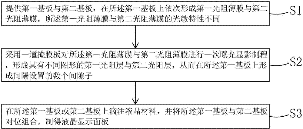
[0042] see figure 1 , the invention provides a method for manufacturing a liquid crystal display panel, comprising the steps of:

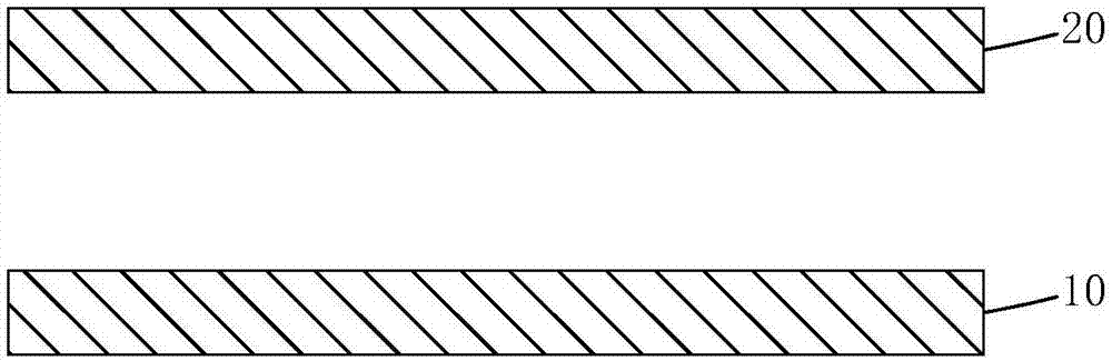
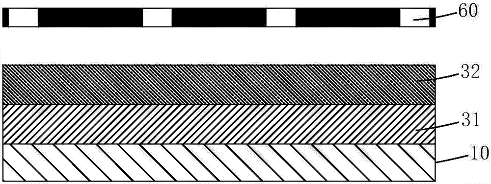
[0043] Step 1, such as figure 2 and image 3 As shown, a first substrate 10 and a second substrate 20 are provided, a first photoresist film 31 is formed on the first substrate 10, and a second photoresist film 32 is formed on the first photoresist film 31; The photosensitive characteristics of the first photoresist film 31 and the second photoresist film 32 are different, that is, the first photoresist film 31 and the second photoresist film 32 have different light reaction absorption wavelengths, or the first photoresist film 31 and the second photoresist film 32 have different photoresponse sensitivities to ...


PUM


Abstract

The invention provides a liquid crystal display panel and a manufacturing method for the same. The manufacturing method for the liquid crystal display panel is that graphical process is conducted to multi-layers of photoresistive films laminated by a common masking plate through a single-exposure development process, and laminated multi-layered photoresist layers can be achieved; photo spacers are formed between the laminated multi-layered photoresist layers; due to the diversities of light-sensitive characteristics of the multi-layered photoresist layers, multi-layered photoresist layers with different graphs can be achieved after exposure development; and the different graphs are different in aspects of at least one parameter such as upper base sizes, lower base sizes, slant angles . Slant angles (Theta) of photo spacers can be adjusted by the multi-layered photoresist layers with different graphs, so the slant angle (Theta) of each photo spacer can be effectively improved; the photo spacers of the liquid crystal display panel has the laminated multi-layered photoresist layers; the multi-layered photoresist layers has different graphs; and the slant angle (Theta) of each photo spacer can be effectively improved.

Description

technical field [0001] The invention relates to the field of display technology, in particular to a liquid crystal display panel and a manufacturing method thereof. Background technique [0002] Liquid crystal display (Liquid Crystal Display, LCD) has many advantages such as thin body, power saving, and no radiation, and has been widely used, such as: mobile phones, personal digital assistants (PDA), digital cameras, computer screens and notebook computers screen etc. [0003] Most of the liquid crystal display devices currently on the market are backlight liquid crystal display devices, which include a backlight module, a liquid crystal panel combined with the backlight module, and a front frame fixing the liquid crystal panel and the backlight module. The working principle of the liquid crystal panel is to place liquid crystal molecules between two parallel glass substrates. There are many vertical and horizontal small wires between the two glass substrates. The direction...

Claims


Application Information

Patent Timeline
Patent Type & Authority Applications(China)
IPC IPC(8): G02F1/1335G02F1/1339G02F1/1362
CPCG02F1/133512G02F1/13394G02F1/136209
Inventor 曹武
Owner SHENZHEN CHINA STAR OPTOELECTRONICS SEMICON DISPLAY TECH CO LTD
Why Eureka
Try Eureka