A TV board test device
A test device and board technology, applied in the field of testing, can solve problems such as waste of resources, irreversible damage to the screen of the whole machine, failure to judge the performance of TV boards, etc., and achieve the effect of solving high costs
- Summary
- Abstract
- Description
- Claims
- Application Information
AI Technical Summary
Problems solved by technology
Method used
Image
Examples
Embodiment 1
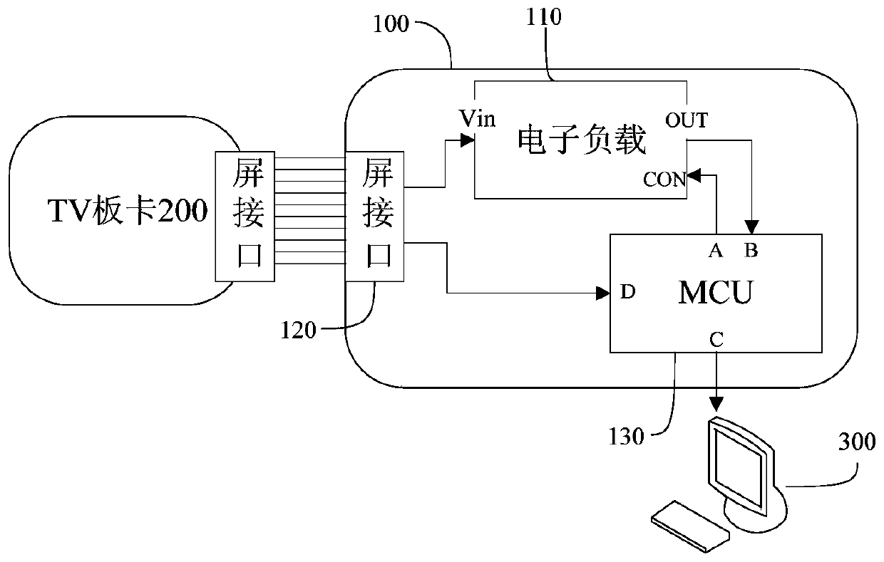
[0020] figure 1 It is a schematic structural diagram of a TV board testing device provided in Embodiment 1 of the present invention. The TV board test device 100 includes: a screen interface 120 , an electronic load 110 and an MCU 130 .
[0021] Among them, the electronic load 110 includes a load regulation terminal CON, a power input terminal Vin and a sampling terminal OUT; the MCU includes a voltage output terminal A, a collection input terminal B, an external communication interface C and a signal detection terminal D.
[0022] The screen interface 120 is used for connecting the TV board 200 to be tested.
[0023] The signal detection terminal D of the MCU 130 is connected to the screen interface to receive the power signal or video signal output by the TV board 200 to be tested.
[0024] The voltage output terminal A of the MCU 130 is connected to the load regulation terminal CON of the electronic load 110, and outputs a control voltage corresponding to the signal recei...
Embodiment 2
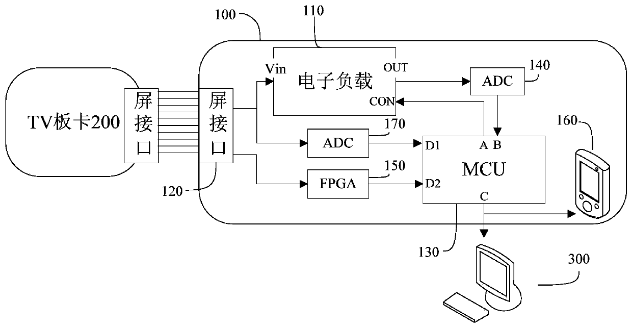
[0031] figure 2 It is a schematic structural diagram of a TV board testing device provided in Embodiment 2 of the present invention. The TV board test device has all the technical features of the TV board test device 100 in Embodiment 1, and also includes: a first ADC collector 140, an FPGA (Field-Programmable Gate Array, Field Programmable Gate Array) 150, The second ADC collector 170 and the display screen 160 . Among them, the ADC collectors 140 and 170 are electronic devices for converting input analog electrical signals into digital electrical signals for output.
[0032] The signal detection terminal D of the MCU 130 in this embodiment receives both the power signal and the video signal from the screen interface, that is, it includes a detection terminal D1 for receiving the power signal and a detection terminal D2 for receiving the video signal. In this embodiment, the MCU 130 judges the type of the whole machine connected to the TV board 200 according to the power s...
Embodiment 3
[0042] Figure 4 It is a schematic structural diagram of a TV board testing device provided in Embodiment 3 of the present invention. The difference between the TV board test device and the TV board test device provided in Embodiment 2 is that in the TV board test device, the signal detection terminal D of the MCU only receives the video signal from the screen interface, and the MCU according to the TV board test device The video signal output by the board judges the type of the whole machine connected when the TV board 200 is used, and outputs a corresponding control voltage. Therefore, compared with the second embodiment, this embodiment omits the first ADC collector 170 . The FPGA is connected between the screen interface 120 and the detection terminal D2 of the MCU, and the video signal of the TV board card to be tested received by the screen interface 120 is formatted and then output to the signal detection terminal D of the MCU, and the MCU outputs the video signal acco...
PUM
 Abstract
Description
Claims
Application Information
 - R&D Engineer
- R&D Manager
- IP Professional
- Industry Leading Data Capabilities
- Powerful AI technology
- Patent DNA Extraction
Browse by: Latest US Patents, China's latest patents, Technical Efficacy Thesaurus, Application Domain, Technology Topic, Popular Technical Reports.
© 2024 PatSnap. All rights reserved.Legal|Privacy policy|Modern Slavery Act Transparency Statement|Sitemap|About US| Contact US: help@patsnap.com


