Broadband confocal waveguide excitation device

A confocal and waveguide technology, applied in waveguide-type devices, circuits, electrical components, etc., can solve the problems of difficult design of 3dB power divider, no mention of 3dB power divider, low bandwidth and coupling efficiency, etc. Practical application value, the effect of reducing diffraction loss and low processing cost

Active Publication Date: 2019-10-01
UNIV OF ELECTRONICS SCI & TECH OF CHINA
View PDF3 Cites 0 Cited by
  • Summary
  • Abstract
  • Description
  • Claims
  • Application Information

AI Technical Summary

Problems solved by technology

Among them, the scheme (1) has the simplest structure, but the bandwidth and coupling efficiency are low. The lowest insertion loss reported in the literature is slightly less than 3dB, and the 3dB bandwidth with a center frequency of 140GHz is about 2GHz; scheme (2) uses two output waveguides of the power splitter Double-fed coupling, symmetrical structure, can suppress some asymmetric modes, Wang Jianxun and others proposed a new type of confocal waveguide broadband input coupling device (patent number: CN201610791802.8), the coupling device adopts double-fed coupling structure, through which The two-way coupling waveguide and the confocal waveguide mirror form an angle of θ, which makes the propagation velocity and group velocity of the microwave propagating in the input waveguide and the confocal waveguide match, effectively solving the problem of narrow bandwidth and low coupling efficiency of the traditional confocal waveguide input structure. 14.08GHz 3dB transmission bandwidth in W band
However, this structure does not mention the design of the 3dB power splitter. Since the device uses an input waveguide inclined to the confocal waveguide, the design of the 3dB power splitter is very difficult and difficult to apply in practice.

Method used


Image

  • Broadband confocal waveguide excitation device
  • Broadband confocal waveguide excitation device
  • Broadband confocal waveguide excitation device

Examples


Embodiment Construction

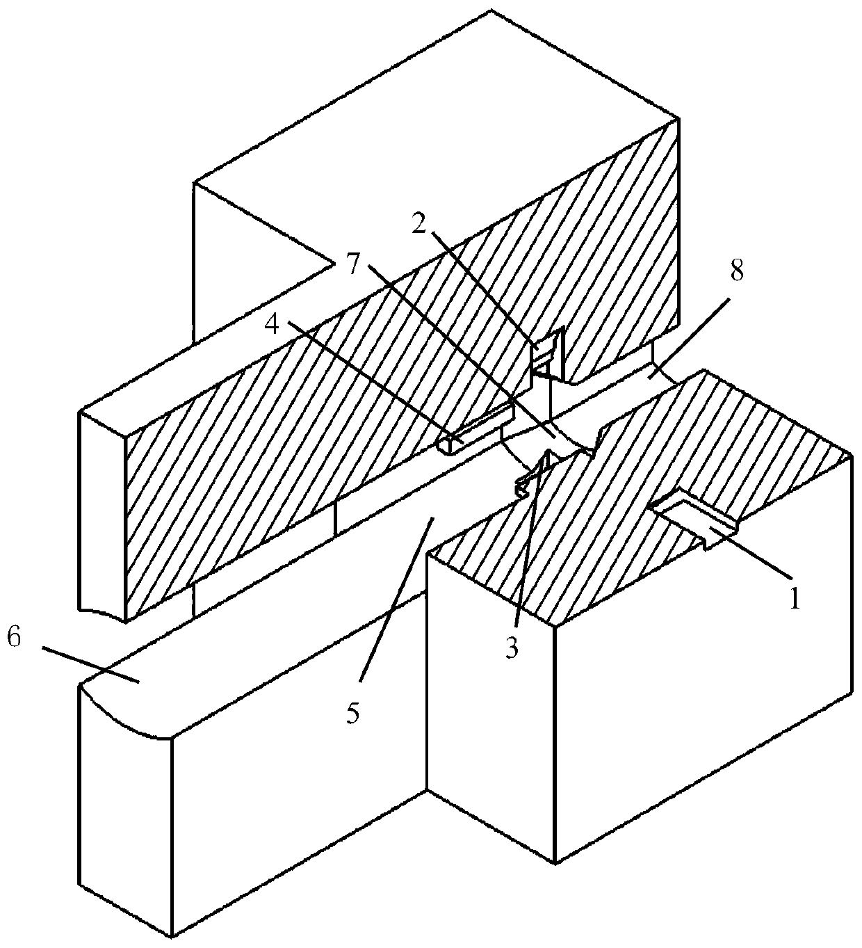
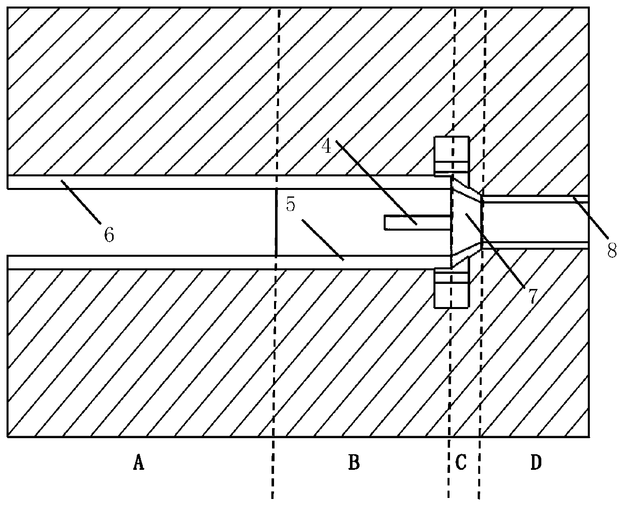
[0027] The following combines a W-band broadband confocal waveguide HE 04 The design examples of the mode excitation device and the accompanying drawings further illustrate the present invention in detail.

[0028] The dispersion characteristic relation of the electromagnetic wave in the confocal waveguide structure is,

[0029] k 2 =k z 2 +k t 2 (1)

[0030] In the above formula k, k z ,k t are the electromagnetic wave number propagating in the confocal waveguide, the longitudinal wave number and the cut-off wave number respectively. According to the confocal waveguide theory, for the HE propagating in the confocal waveguide mn Mode (m, n are the mode labels in the x direction and y direction respectively) electromagnetic wave, its cut-off wave number k t satisfy:

[0031] k t =k tr +jk ti (2)

[0032]

[0033] where k t is the cut-off wave number, the real part k tr and imaginary part k ti The transmission characteristics and diffraction loss characteri...


PUM


Abstract

The invention discloses a broadband confocal waveguide HE0n mode excitation device, which belongs to the technical field of vacuum electronics. The device includes an output open confocal waveguide section, a closed confocal waveguide mode conversion section, a cut-off gradient section, and a uniform open waveguide in the cut-off section; a Y-shaped 3dB power splitter is provided at the junction of the closed confocal waveguide mode conversion section and the cut-off gradient section. The two output waveguides are bent inward at 90 degrees and are perpendicular to the input waveguide, and the output port obtains two microwave signals of equal amplitude and opposite directions. The invention adopts a double-fed structure perpendicular to the confocal waveguide mirror surface, and realizes the high-efficiency conversion of the HE0n mode of the confocal waveguide within a broadband range through two pairs of reflective mirror surfaces in the cut-off transition section, and the band is flat. It can be realized by traditional processing methods in the millimeter wave and terahertz frequency bands; the sensitivity of the structural parameters is low, and it can be directly applied to the input coupling device of the confocal waveguide cyclotron amplifier device, the cyclotron oscillator device and the cyclotron amplifier in the millimeter wave and terahertz frequency bands Cold test experiment of high-frequency system characteristics of components.

Description

technical field [0001] The invention belongs to the technical field of vacuum electronics, and in particular relates to a confocal waveguide mode excitation device applied to confocal waveguide gyro devices in the millimeter wave and terahertz bands. Background technique [0002] Gyrotron is an important millimeter wave-terahertz radiation source device, which has important applications in controlled nuclear fusion, plasma heating, plasma diagnosis, radar system, communication and electronic countermeasures, industrial processing, etc. The confocal waveguide gyro device adopts a new type of confocal waveguide interaction structure, which has good mode selection characteristics compared with the traditional cylindrical waveguide gyrotron, and effectively solves the problem of too small lateral size and the Due to the low average power capacity, severe electron beam interception and processing difficulties, it has important application prospects in the terahertz frequency band...

Claims


Application Information

Patent Timeline
Patent Type & Authority Patents(China)
IPC IPC(8): H01P1/163
Inventor 王建勋姚叶雷罗勇
Owner UNIV OF ELECTRONICS SCI & TECH OF CHINA
Why Eureka
Try Eureka