An organic light emitting display panel
A technology of light-emitting display and organic light-emitting layer, which is applied in the direction of semiconductor devices, electrical components, circuits, etc., can solve the problems of reducing panel display quality and light leakage, and achieve the effect of improving display quality and suppressing the path of lateral conduction
- Summary
- Abstract
- Description
- Claims
- Application Information
AI Technical Summary
Problems solved by technology
Method used
Image
Examples
Embodiment Construction
[0018] The present invention will be described in detail below in conjunction with the accompanying drawings and embodiments.
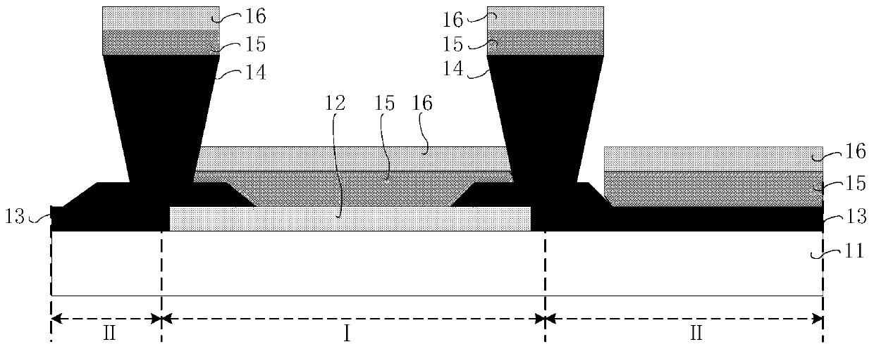
[0019] see figure 1 , figure 1 It is a schematic structural view of the first embodiment of the organic light emitting display panel of the present invention. Such as figure 1 As shown, the organic light emitting display panel 10 of this embodiment includes: a substrate 11 , an anode electrode 12 , a pixel definition layer 13 , an isolation pattern 14 , an organic light emitting layer 15 and a cathode layer 16 . Wherein, the organic light emitting display panel 10 is divided into an effective light emitting area I and an ineffective light emitting area II, the effective light emitting area I corresponds to the anode electrode 12, and the ineffective light emitting area II is located around the effective light emitting area. Specifically, there are a plurality of anode electrodes 12, all of which are formed on the substrate 11 in an array; the pixel...
PUM
 Abstract
Description
Claims
Application Information
 - R&D
- Intellectual Property
- Life Sciences
- Materials
- Tech Scout
- Unparalleled Data Quality
- Higher Quality Content
- 60% Fewer Hallucinations
Browse by: Latest US Patents, China's latest patents, Technical Efficacy Thesaurus, Application Domain, Technology Topic, Popular Technical Reports.
© 2025 PatSnap. All rights reserved.Legal|Privacy policy|Modern Slavery Act Transparency Statement|Sitemap|About US| Contact US: help@patsnap.com


