Chip bonding apparatus and method

A chip bonding and chip technology, which is used in transportation and packaging, semiconductor devices, electrical components, etc., can solve the problems of low yield, low yield of flip-chip bonding devices, and difficulty in meeting mass production requirements, so as to improve efficiency. , Improve the yield and ensure the effect of bonding accuracy

Active Publication Date: 2020-05-01
SHANGHAI MICRO ELECTRONICS EQUIP (GRP) CO LTD
View PDF5 Cites 0 Cited by
  • Summary
  • Abstract
  • Description
  • Claims
  • Application Information

AI Technical Summary

Problems solved by technology

However, because the existing flip-chip bonding device can only bond one chip at a time (about 30 seconds), the entire process is completed in series, so the yield is very low, and it is difficult to meet the needs of mass production.
[0005] Based on this, how to improve the low yield of flip-chip bonding devices in the prior art and the difficulty in meeting mass production requirements has become a technical problem that those skilled in the art need to solve urgently.

Method used


Image

  • Chip bonding apparatus and method
  • Chip bonding apparatus and method
  • Chip bonding apparatus and method

Examples


Embodiment Construction

[0040] The present invention will be described in further detail below in conjunction with the accompanying drawings and specific embodiments. Advantages and features of the present invention will be apparent from the following description and claims. It should be noted that the drawings are all in a very simplified form and use imprecise ratios, which are only used to facilitate and clearly assist the purpose of illustrating the embodiments of the present invention.

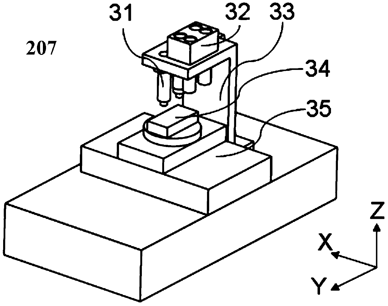
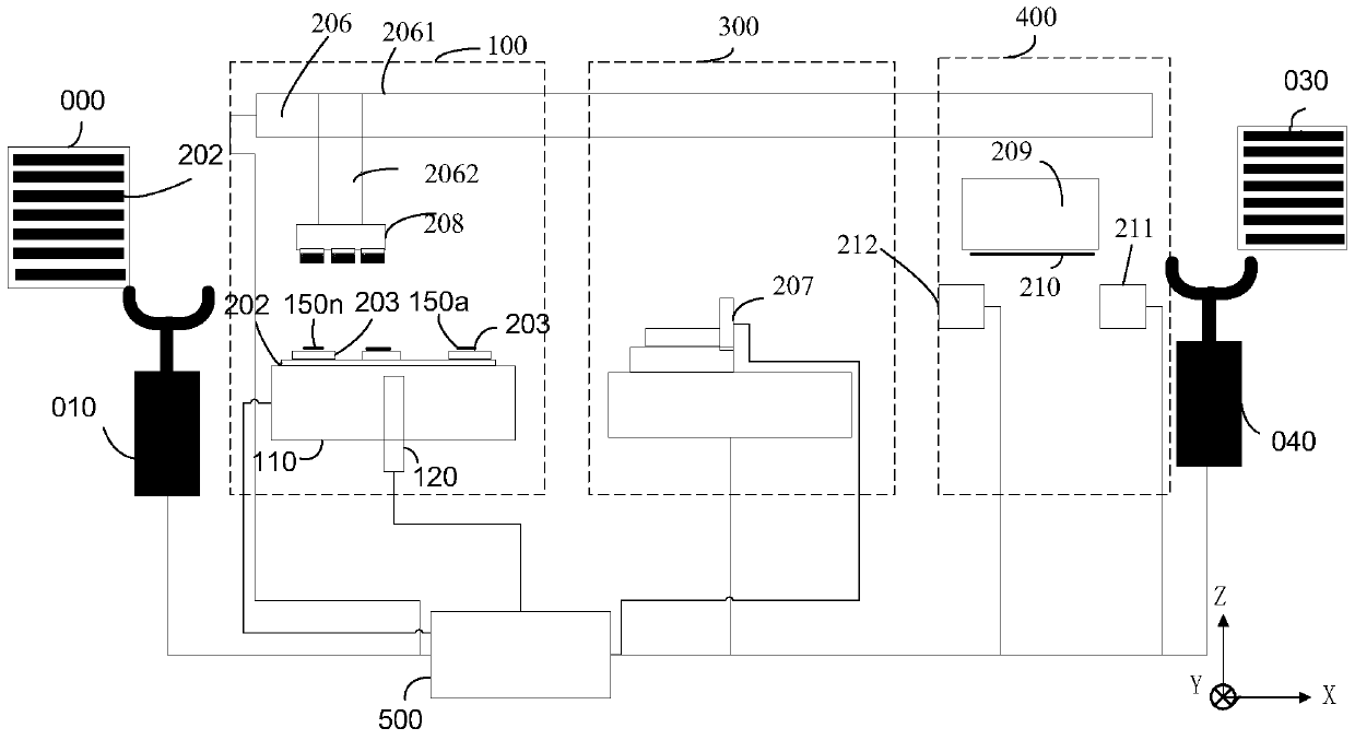
[0041] Such as image 3 As mentioned above, the structure of the chip bonding device involved in the embodiment of the present invention includes: the first moving table 110, the second moving table 206, the suction cup 208, the fine adjustment and transfer structure 207, the bonding table 209 and the control system 500;

[0042] The first moving platform 110 is used to carry and transport the chipset to a predetermined pick-up position;

[0043] The second moving table 206 is used to drive the suction cup 208...


PUM


Abstract

The invention provides a chip bonding device which comprises a first moving table, a second moving table, an absorbing disc, an accurate adjustment and transfer structure, a bonding table and a control system. The invention further provides a chip bonding method, which is characterized in that chips are absorbed one by one through adopting the absorbing disc, then the position of each chip on a carrier plate is accurately adjusted through the accurate adjustment and transfer structure, and the chips on the carrier plate are bonded to a substrate in one time, so that batch bonding of the chips is realized, and the efficiency of a flip chip bonding process is effectively improved. The chip bonding device adopts a mode of chip batch pickup and batch bonding, the time of chip pickup, chip position accurate adjustment and chip bonding is balanced, the bonding device is enabled to improve the yield while ensuring the bonding precision.

Description

technical field [0001] The invention relates to the technical field of chip packaging, in particular to a chip bonding device and method. Background technique [0002] With the development of science and technology, electronic products are increasingly developing in the direction of lightness, thinness and miniaturization. Since the flip-chip bonding technology has many advantages such as reducing the chip packaging area and shortening the signal transmission path, it has been widely used in the field of chip packaging. [0003] Please refer to figure 1 , which is a schematic diagram of chip bonding performed by a flip chip bonding device in the prior art. Such as figure 1 As shown, the existing flip-chip bonding process mainly includes the following steps: first, a chip 2 and a substrate 4 to be bonded are provided, and the chip 2 has a device face 3; then, the chip 2 is placed with the device face 3 upward Then, use the first manipulator 5 to grab the chip 2 and turn i...

Claims


Application Information

Patent Timeline
Patent Type & Authority Patents(China)
IPC IPC(8): H01L21/673H01L21/677H01L21/60H01L21/67
CPCH01L21/67H01L21/673H01L21/677H01L24/01
Inventor 郭耸朱岳彬陈飞彪戈亚萍
Owner SHANGHAI MICRO ELECTRONICS EQUIP (GRP) CO LTD
Why Eureka
Try Eureka