
Organic light-emitting device

一种电致发光器件、致发光的技术,应用在电固体器件、电气元件、半导体器件等方向,能够解决选择范围小等问题,达到降低工作电压、提高显示性能、简化器件结构的效果

Active Publication Date: 2017-07-04
KUNSHAN NEW FLAT PANEL DISPLAY TECH CENT
View PDF6 Cites 10 Cited by
  • Summary
  • Abstract
  • Description
  • Claims
  • Application Information

AI Technical Summary

Problems solved by technology

[0006] Therefore, what the present invention aims to solve is the problem that the combination selection range of luminescent materials in the existing organic electroluminescent device sharing the blue light layer is small, thereby providing a red / green sub-pixel emission spectrum that does not contain blue light, and the combination selection of luminescent materials Large-range shared blue-light layer organic electroluminescent devices

Method used


Image

  • Organic light-emitting device
  • Organic light-emitting device
  • Organic light-emitting device

Examples


Embodiment 1

[0045] This embodiment provides an organic electroluminescent device, such as figure 1 As shown, it includes the first electrode 2, the first light emitting layer 3, the second light emitting layer 4 and the second electrode 5 stacked on the substrate 1; the first light emitting layer 3 includes several red light units 301 arranged on the same layer , several green light units 302 and several blue light units 303, the second light emitting layer 4 is a blue light layer. In this embodiment, preferably, the blue light unit 303 in the first light-emitting layer 3 is made by extending the second light-emitting layer 4 to the first light-emitting layer 3, that is, the material of the blue light unit 303 and the The materials of the second light-emitting layer 4 are consistent.

[0046] As an alternative embodiment of the present invention, the material of the blue light unit 303 may also be different from that of the second light-emitting layer 4 , both of which can achieve the p...

Embodiment 2

[0053] This embodiment provides an organic electroluminescence device, the device structure is the same as that of Embodiment 1, the difference is that the host material in the red light unit 301 is the thermally activated delayed fluorescent material shown in formula (1-1) and the The host material in the green light unit 302 is the thermally activated delayed fluorescent material shown in formula (1-2).

Embodiment 3

[0055] This embodiment provides an organic electroluminescence device, the structure of which is the same as that of Embodiment 1, except that the host material in the green light unit 302 is a thermally activated delayed fluorescent material represented by formula (1-11).


PUM


Abstract

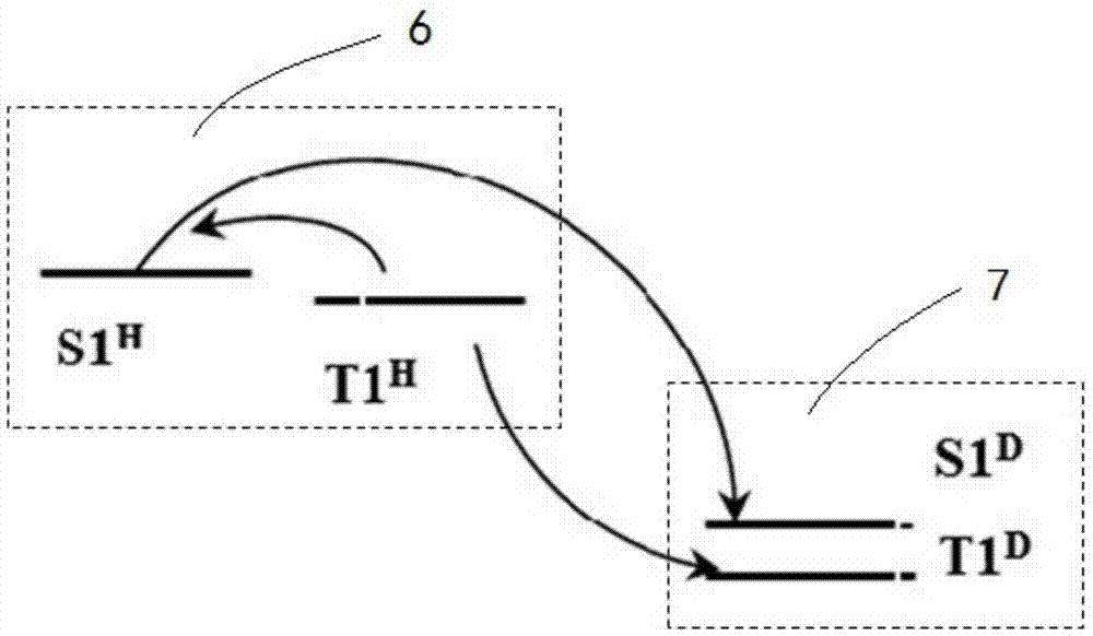
The invention discloses an organic light-emitting device. According to the organic light-emitting device, a TADF material is used as a first host material of a green light unit to sensitize a green phosphorescent material used as a first guest material. Partial triplet excitons are subjected to reverse intersystem crossing to singlet excitons. The concentration of the triplet excitons decreases to enable a recombination region to become narrow, which avoids the diffusion of the triplet excitons to a blue light layer to emit light so as to realize that the green spectrum does not contain a blue light component. Because the energy level difference between the red light and the blue light is relatively large, and current carriers in the red light are not liable to spread into the blue light, the blue light component is not liable to appear in the red spectrum. Therefore, the red / green subpixel emission spectrum in a blue-light-layer-shared organic light-emitting device does not contain the blue light, which can effectively enlarge the combination selection range of luminescent materials and improve the display performance of the device. In addition, there is no need for providing a hole blocking layer, and the device structure is effectively simplified, so that operating voltage is reduced; and meanwhile, the difficulty of the process is reduced, and product yield is improved, so that production cost is reduced.

Description

technical field [0001] The invention relates to the field of organic electroluminescence, in particular to an organic electroluminescence device and a preparation method thereof. Background technique [0002] Organic electroluminescent device (English full name Organic Light-Emitting Device, referred to as OLED) adopts organic electroluminescent material, is an active light-emitting device, has the advantages of low power consumption, wide color gamut, and thinner volume, and is expected to become the next generation of mainstream lighting and flat panel display technology. [0003] At present, organic electroluminescent display technology has been widely used in small-sized panels such as smartphone display screens. At this stage, there are three main ways for organic electroluminescent display devices to realize full-color display: one is the primary color pixel juxtaposition method, which represents P (full name in English called Pentile, translated as waveform) arrangem...

Claims


Application Information

Patent Timeline
Patent Type & Authority Applications(China)
IPC IPC(8): H01L51/50H01L51/54
CPCH10K85/654H10K50/121H10K50/11H10K2101/10H10K59/35H10K50/13H10K2101/20H10K59/00H10K50/00H10K50/15H10K50/167
Inventor 高松刘嵩赵菲
Owner KUNSHAN NEW FLAT PANEL DISPLAY TECH CENT
Learn More