FC-AE-1553 simulation communication demonstration system and data transmission method
A demonstration system and communication card technology, applied in the transmission system, digital transmission system, data exchange network, etc., can solve the problems that cannot fully meet the various technical indicators of the spacecraft
- Summary
- Abstract
- Description
- Claims
- Application Information
AI Technical Summary
Problems solved by technology
Method used
Image
Examples
Embodiment 1
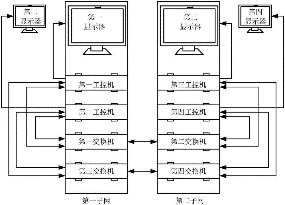
[0115] figure 1 A schematic diagram of the structure of the FC-AE-1553 simulation communication demonstration system provided by the embodiment of the present invention.
[0116] The embodiment of the invention provides a simulation communication demonstration system suitable for the FC-AE-1553 high-speed bus protocol. Described emulation communication demonstration system adopts the frame-mounted structure of cabinet to form, and this emulation demonstration system is mainly made up of 2 independent cabinets, and each cabinet forms a subnet corresponding to FC-AE-1553 bus network (such as figure 1 The first subnet and the second subnet shown in ), the embodiment of the present invention adopts a switched networking structure to build a FC-AE-1553 dual redundant network.
[0117] Such as figure 1 As shown, the simulation communication demonstration system of the embodiment of the present invention is composed of 4 monitors, 4 industrial computers (including keyboards and mic...
Embodiment 2
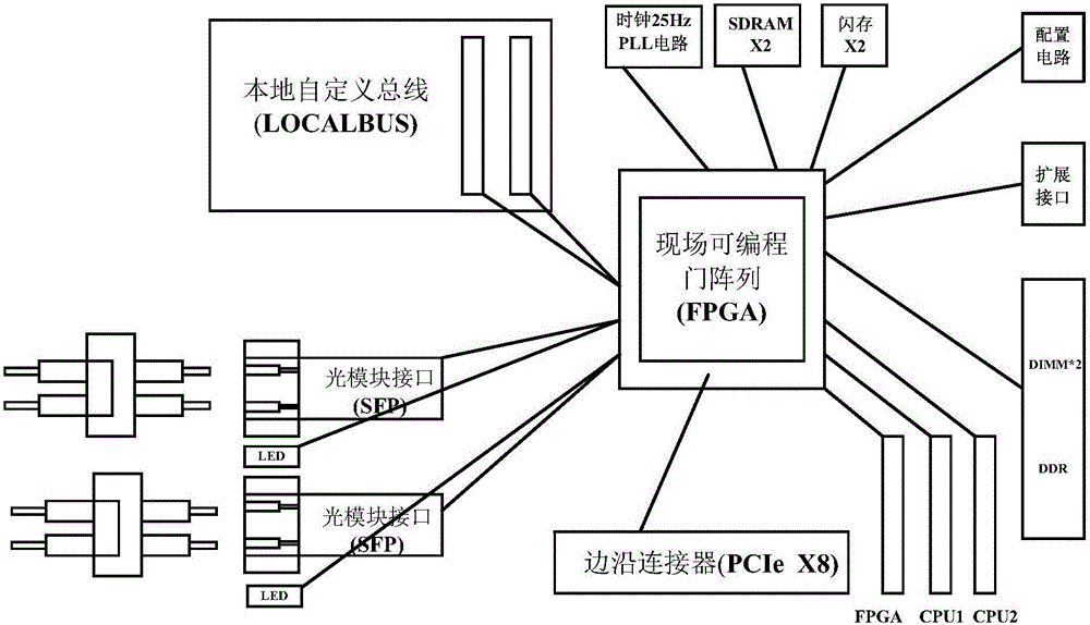
[0149] figure 2 The structural diagram of the FC-AE-1553 emulation communication card provided for the embodiment of the present invention, such as figure 2 As shown, the simulated communication card provided in this embodiment includes:
[0150] FPGA (Field-Programmable Gate Array, Field Programmable Gate Array) unit is used to realize the control logic function according to the preset application requirements;
[0151] The optical module interface unit SFP is used to send and receive link optical signals, and convert the received optical signals into serial digital signals for processing by the FPGA unit, and at the same time convert the serial digital signals from the FPGA unit into optical signals and send them to the optical fiber link road;
[0152] Edge connector, one end is connected to the PCI-E (bus interface) slot of the host computer backplane where the emulation communication card is inserted, and the other end is connected to the encoding module GTX interface...
Embodiment 3
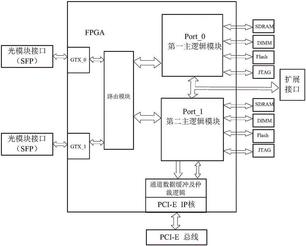
[0167] refer to image 3 As shown, it is a schematic structural diagram of the FPGA unit provided by the embodiment of the present invention. The communication card provided by the embodiment of the present invention adopts a dual optical port and dual channel structure design. Therefore, the FPGA unit contains two sets of main logic modules, corresponding to two channels (Port_0 and Port_1), such as image 3 As shown, the two sets of main logic modules are respectively the first main logic module Port_0 and the second main logic module Port_1, and the internal logics of the two sets of main logic modules are completely the same. In addition to the above two main logic modules, the FPGA unit also includes a routing module and a PCI-E IP core module for communication between the board hardware and the host computer; it also includes channel data corresponding to the PCI-E core Buffer and arbitration logic module; also includes two GTX modules (the first encoding module GTX_0 ...
PUM
 Abstract
Description
Claims
Application Information
 - Generate Ideas
- Intellectual Property
- Life Sciences
- Materials
- Tech Scout
- Unparalleled Data Quality
- Higher Quality Content
- 60% Fewer Hallucinations
Browse by: Latest US Patents, China's latest patents, Technical Efficacy Thesaurus, Application Domain, Technology Topic, Popular Technical Reports.
© 2025 PatSnap. All rights reserved.Legal|Privacy policy|Modern Slavery Act Transparency Statement|Sitemap|About US| Contact US: help@patsnap.com


