


Quick Research
Generate reliable direction feasibility study reports for your R&D in just a few steps.

Technical Q&A
Discover and master advanced knowledge NOW. Basics, ideas, possibilities, all at once.

Find Solutions
As an expert in R&D theories, this can generate solutions to your technical problems instantly.

Evaluate Feasibility
Analyze your overall solution with one click, know your potential R&D risks in advance.

Monitor Landscape
Get weekly tech updates, stay abreast of the latest tech innovations and key insights.
Mask plate, display substrate and manufacturing method thereof
A technology for a display substrate and a mask plate, which is applied in the field of display substrate and its fabrication and mask plate, can solve the problems of long development cycle and high production cost, and achieve the effect of reducing production cost and shortening development cycle.
- Summary
- Abstract
- Description
- Claims
- Application Information
AI Technical Summary
Problems solved by technology
Method used
Image

Examples
Embodiment 1
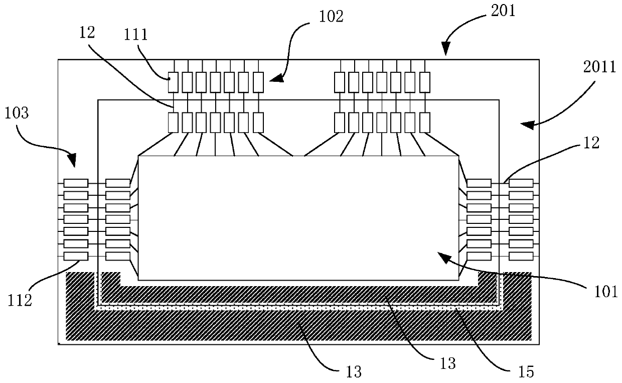
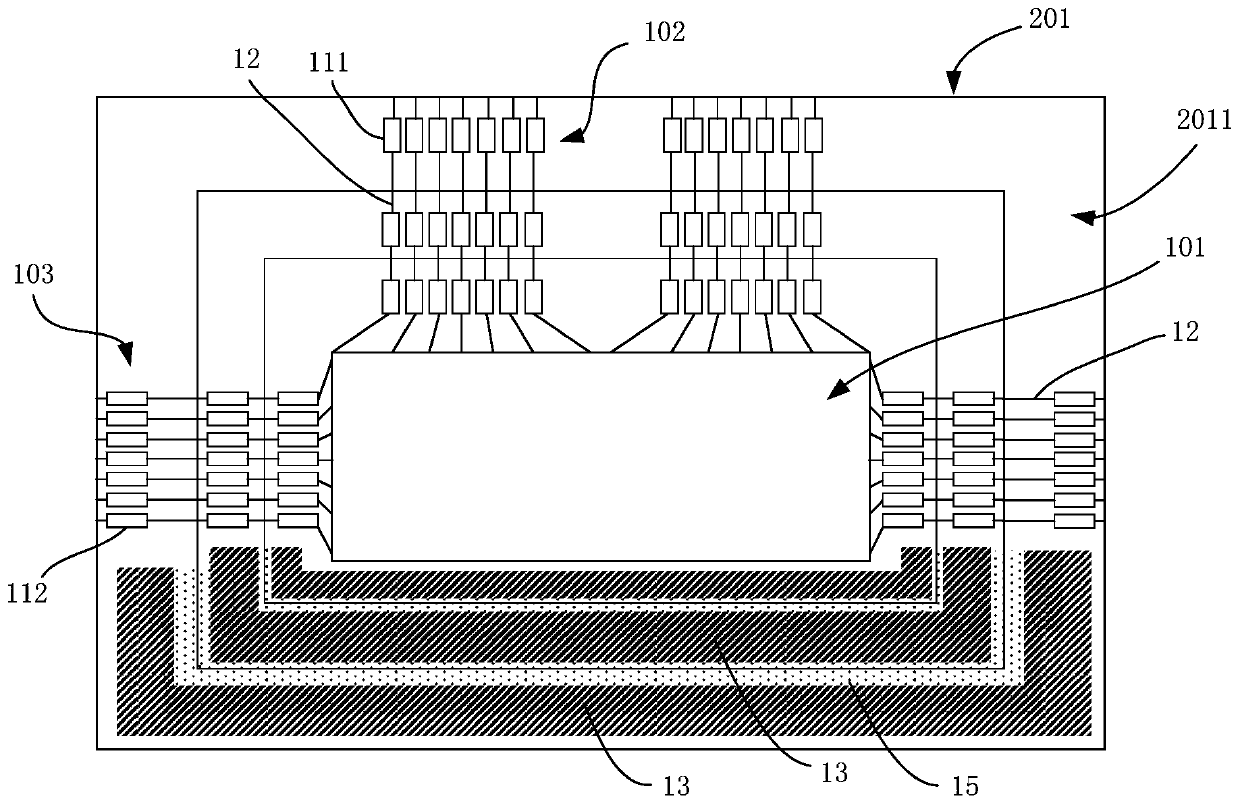
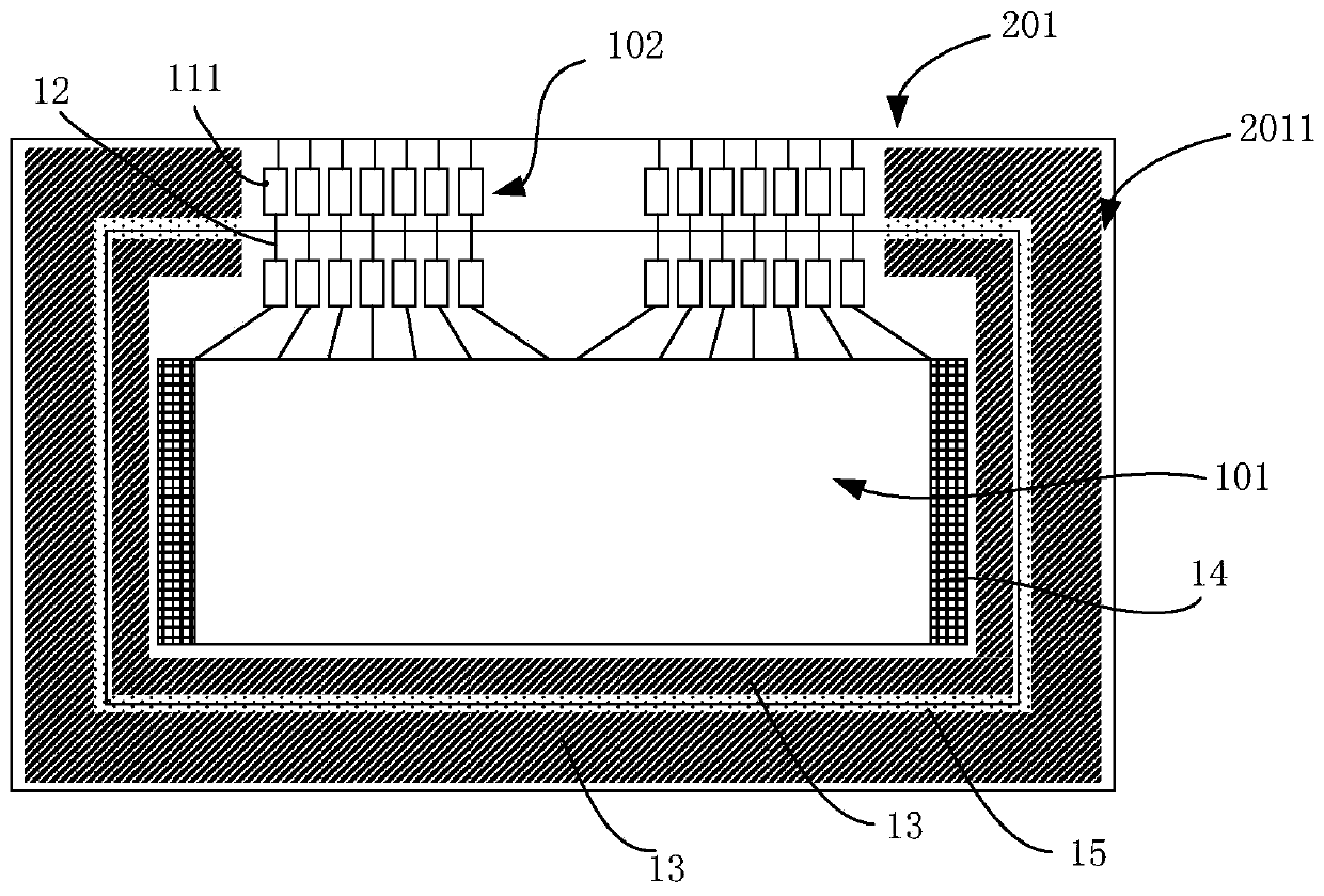
[0026] In this embodiment, a mask plate is provided for making a display substrate, and the same mask plate substrate can be used to complete the manufacture of display substrates of various sizes and specifications, wherein the display area of the display substrates of different sizes and specifications same.
[0027] It should be noted that the same display area refers to the same display area of the display substrate. Different size specifications mean that the areas of the non-display regions of the display substrates are different. In the following content, unless otherwise stated, different dimensions refer to different areas of the non-display area of the display substrate.
[0028] to combine Figure 1-Figure 4 As shown, the mask includes a first region 101 and a second region 201 surrounding the first region 101 . The first area 101 is used for making the display area of the display substrate, including mask patterns (not shown in the figure) used for makin...
Embodiment 2
[0048] combine Figure 5 and Figure 6 As shown, this embodiment provides a display substrate manufactured by using the mask plate in Embodiment 1, and the display substrate includes a display area 100 and a non-display area 200 surrounding the display area 100 .
[0049] The non-display area 200 is divided into at least two ring-shaped sub-non-display areas 2001. For the display substrate, display substrates of different sizes and specifications can be obtained, wherein the display substrates of different sizes and specifications share a display area 100 and have the same display area.
[0050] The sub-non-display area 2001 includes at least one terminal area, each terminal area is provided with a plurality of terminals, and the number of terminals can be set according to the resolution and size of the product. The non-display area 200 further includes a plurality of first bridge lines 2 , and the first bridge lines 2 extend from one sub-non-display area 2001 to another adj...
PUM
 Abstract
Description
Claims
Application Information
 - R&D Engineer
- R&D Manager
- IP Professional
- Industry Leading Data Capabilities
- Powerful AI technology
- Patent DNA Extraction
Browse by: Latest US Patents, China's latest patents, Technical Efficacy Thesaurus, Application Domain, Technology Topic, Popular Technical Reports.
© 2024 PatSnap. All rights reserved.Legal|Privacy policy|Modern Slavery Act Transparency Statement|Sitemap|About US| Contact US: help@patsnap.com