Pixel structure of liquid crystal display panel and display device

A liquid crystal display panel and pixel structure technology, applied in nonlinear optics, instruments, optics, etc., can solve problems such as large viewing angle deviation, achieve the effect of reducing loading time and improving charging conditions

Active Publication Date: 2017-05-31
TCL CHINA STAR OPTOELECTRONICS TECH CO LTD
View PDF7 Cites 4 Cited by
  • Summary
  • Abstract
  • Description
  • Claims
  • Application Information

AI Technical Summary

Problems solved by technology

[0008] The object of the present invention is to provide a pixel structure and a display device of a liquid crystal display panel, so as to solve the problem of large viewing angle deviation in the liquid crystal display panel in the prior art

Method used


Image

  • Pixel structure of liquid crystal display panel and display device
  • Pixel structure of liquid crystal display panel and display device
  • Pixel structure of liquid crystal display panel and display device

Examples


Embodiment 1

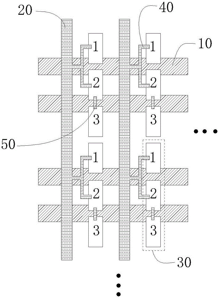
[0032] Please refer to figure 1 , figure 1 It is a schematic diagram of the overall structure of a pixel structure of a liquid crystal display panel in this embodiment.

[0033] From figure 1 It can be seen that a pixel structure of a liquid crystal display panel of the present invention includes a plurality of data lines 20, a plurality of gate lines 10 and a plurality of pixel units 30 arranged in multiple columns, and each of the pixel units 30 includes The first luminance area 1, the second luminance area 2 and the third luminance area 3 are vertically arranged. In one pixel unit 30, the first luminance area 1 and the second luminance area 2 are the same A first switch 40 is provided between the data lines 20 , and a second switch 50 is provided between the second brightness area 2 and the third brightness area 3 . Wherein, both the first switch 40 and the second switch 50 in this embodiment are TFT switches, that is, thin film transistor switches.

[0034] Wherein, in...

Embodiment 2

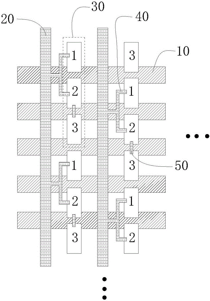
[0049] This embodiment provides a display device, which includes a liquid crystal display panel, and the liquid crystal display panel includes the pixel structure described in the first embodiment. The pixel structure has been described in detail in Embodiment 1, and will not be discussed here again.

[0050] A display device of the present invention, which includes a liquid crystal display panel, the liquid crystal display panel includes a pixel structure, the pixel structure is designed by designing each pixel unit 30 into a first brightness region 1, a second brightness region 2 and a third brightness region In the brightness area 3, each brightness area is provided with 4 domains, and in a pixel unit 30, a first switch 40 is respectively provided between the first brightness area 1 and the second brightness area 2 and the same data line 20, and the second A second switch 50 is provided between the second brightness region 2 and the third brightness region 3, and in the sam...


PUM


Abstract

The invention provides a pixel structure of a liquid crystal display panel and a display device. The pixel structure comprises multiple data lines, multiple gate lines and multiple pixel units arrayed in multiple columns, each pixel unit comprises a first brightness area, a second brightness area and a third brightness area in vertical array, in one pixel unit, a first switch is arranged between the first brightness area and the same data line as well as between the second brightness area and the same data line, and a second switch is arranged between the second brightness area and the third brightness area. In the same pixel unit, the gate line controlling the two first switches and the gate line controlling the second switches are two adjacent gate lines. The problem that large viewing-angle color cast of the liquid crystal display panel in the prior art is solved.

Description

[0001] 【Technical field】 [0002] The invention relates to the technical field of liquid crystal display panels, in particular to a pixel structure of a liquid crystal display panel and a display device. [0003] 【Background technique】 [0004] The liquid crystal display panel industry has experienced decades of development. The VA (vertical alignment) display mode has become a common display mode for large-size TV TFT-LCDs due to its advantages such as wide viewing angle, high contrast, and no need for frictional alignment. However, compared with the IPS (In-Plane Switching) display mode, its viewing angle performance is not satisfactory. Therefore, the multi-domain structure has become the main means to improve the problem of large-view role deviation in the VA display mode. [0005] Pixels with a multi-domain structure are usually divided into a Main area and a Sub area. At the same time, the pixel voltage of the Sub area is required to be lower than that of the Main area, s...

Claims


Application Information

Patent Timeline
IPC IPC(8): G02F1/1362
CPCG02F1/13624G02F1/136286
Inventor 陈帅
Owner TCL CHINA STAR OPTOELECTRONICS TECH CO LTD
Why Eureka
Try Eureka