Packaging technique of LED display screen module
A technology of LED display and packaging technology, which is applied in the direction of identification devices, instruments, electrical components, etc., which can solve the problems of low resolution and insufficient display effect, so as to improve the resolution, display better and more delicate, and increase the unit area pixel effect
- Summary
- Abstract
- Description
- Claims
- Application Information
AI Technical Summary
Problems solved by technology
Method used
Image
Examples
Embodiment Construction
[0019] In conjunction with the accompanying drawings, the specific implementation manners of the present invention will be further described in detail, so as to make the technical solution of the present invention easier to understand and grasp.
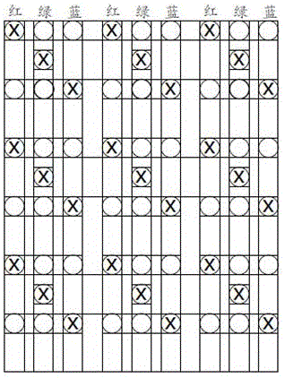
[0020] A packaging process for an LED display module, comprising the following steps:
[0021] 1) The red, blue and green display chips are sealed on the surface of the colloid according to the law;
[0022] 2) Plating the first layer of conductive film on the back of the red, blue and green display chips, and carving off the excess film to form the required conductive lines, so that the chips are connected in series;
[0023] 3) Cover a protective layer on the first layer of conductive film, and engrave off the protective layer of the first chip pad (BOND PAD) to expose the pad;
[0024] 4) Plating a second layer of conductive film on the protective layer, and carving off the excess film to form the required conductive line, and to...
PUM
 Abstract
Description
Claims
Application Information
 - R&D
- Intellectual Property
- Life Sciences
- Materials
- Tech Scout
- Unparalleled Data Quality
- Higher Quality Content
- 60% Fewer Hallucinations
Browse by: Latest US Patents, China's latest patents, Technical Efficacy Thesaurus, Application Domain, Technology Topic, Popular Technical Reports.
© 2025 PatSnap. All rights reserved.Legal|Privacy policy|Modern Slavery Act Transparency Statement|Sitemap|About US| Contact US: help@patsnap.com

