PCB laminate process and PCB
A process and multi-layer board technology, applied in the direction of lamination, lamination device, layered products, etc., can solve the problems of different degrees of board surface warpage, temperature difference, unstable reliability, etc., to ensure stability, layer The pressure state is consistent and the effect of improving the material temperature difference
- Summary
- Abstract
- Description
- Claims
- Application Information
AI Technical Summary
Problems solved by technology
Method used
Image
Examples
Embodiment 1
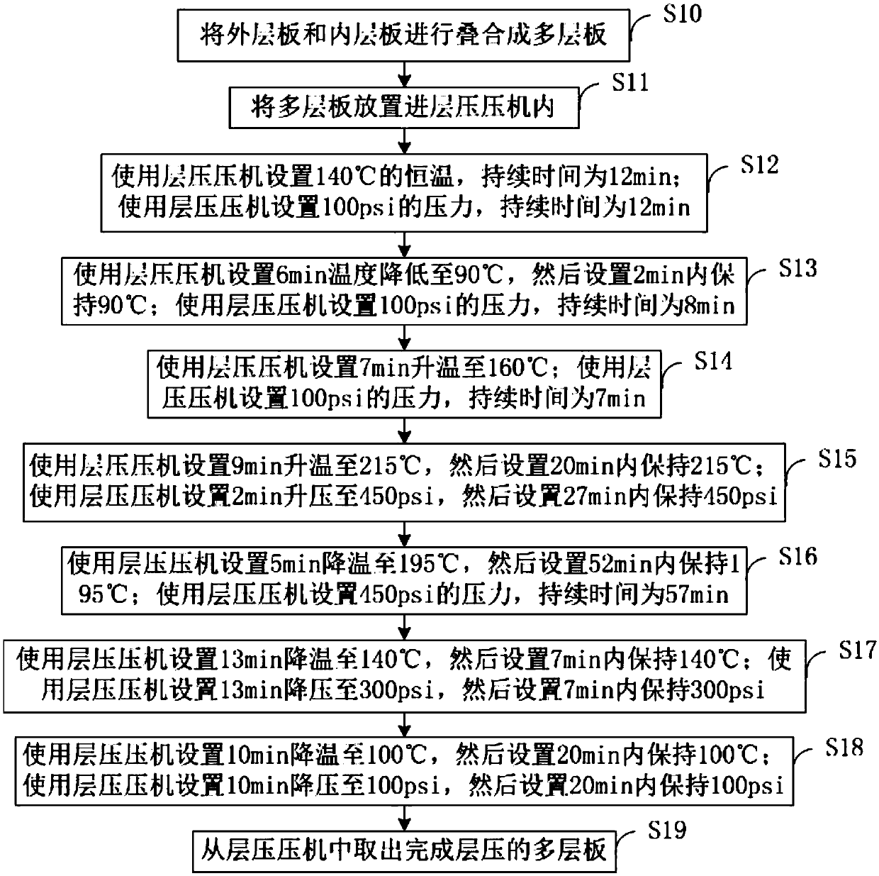
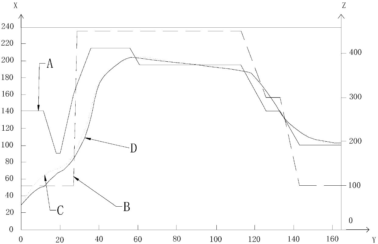
[0043] as table 1 and figure 2 As shown, in this embodiment, a laminated board process for PCB includes the following steps:
[0044] placing the stacked multilayer boards under constant temperature and constant pressure conditions of a first temperature value and a first pressure value, and heating up the multilayer boards after a first time interval;
[0045] Lowering the temperature to a second temperature value, the second temperature value being lower than the first temperature value, placing the multi-layer board under constant temperature and constant pressure conditions of the second temperature value to raise the temperature of the multi-layer board after a second time interval;
[0046] Increase the temperature and pressure to press the multi-layer board.
[0047] In this embodiment, the material of the multilayer board is common FR-4. The melting temperature of the material resin is between 70°C and 80°C.
[0048] In this embodiment, the temperature is lowered t...
Embodiment 2
[0084] The difference between this embodiment and Embodiment 1 is:
[0085] The laminated board process of the PCB, the specific steps are as follows:
[0086] S20, stacking the outer layer board and the inner layer board to form a multi-layer board.
[0087] S21. Put the multi-layer board into the lamination press.
[0088] S22. Use the lamination press to set a constant temperature of 135° C. for 10 minutes; use the lamination press to set a pressure of 95 psi for 10 minutes.
[0089] S23. Use the lamination press to lower the temperature to 85° C. for 5 minutes, and then keep it at 85° C. for 1 minute; use the lamination press to set a pressure of 95 psi for 6 minutes.
[0090] S24. Use the lamination press to set the temperature to 150° C. for 6 minutes; use the lamination press to set a pressure of 95 psi for 6 minutes.
[0091] S25. Use the lamination press to set the temperature to 210°C for 8 minutes, and then set it to maintain 210°C for 18 minutes; use the laminat...
Embodiment 3
[0097] The difference between this embodiment and Embodiment 1 is:
[0098] The laminated board process of the PCB, the specific steps are as follows:
[0099] S30 , stacking the outer layer board and the inner layer board to form a multilayer board.
[0100] S31. Put the multi-layer board into the lamination press.
[0101] S32. Use the lamination press to set a constant temperature of 145° C. for 14 minutes; use the lamination press to set a pressure of 105 psi for 14 minutes.
[0102] S33. Use the lamination press to lower the temperature to 95° C. for 7 minutes, and then maintain the temperature at 95° C. for 3 minutes; use the lamination press to set a pressure of 95 psi for 10 minutes.
[0103] S34. Use a lamination press to set the temperature to 170° C. for 8 minutes; use a lamination press to set a pressure of 95 psi for 8 minutes.
[0104] S35. Use the lamination press to set the temperature to 220°C for 10 minutes, and then set it to maintain 220°C for 22 minutes...
PUM
| Property | Measurement | Unit |
|---|---|---|
| melting point | aaaaa | aaaaa |
Abstract
Description
Claims
Application Information
 - R&D
- Intellectual Property
- Life Sciences
- Materials
- Tech Scout
- Unparalleled Data Quality
- Higher Quality Content
- 60% Fewer Hallucinations
Browse by: Latest US Patents, China's latest patents, Technical Efficacy Thesaurus, Application Domain, Technology Topic, Popular Technical Reports.
© 2025 PatSnap. All rights reserved.Legal|Privacy policy|Modern Slavery Act Transparency Statement|Sitemap|About US| Contact US: help@patsnap.com


