Display panel, manufacturing method thereof and display device
A technology for display panels and manufacturing methods, applied in semiconductor/solid-state device manufacturing, semiconductor devices, electrical components, etc., can solve problems such as leaks, achieve the effects of improving stability, increasing length, and slowing down the rate of water and oxygen penetration
- Summary
- Abstract
- Description
- Claims
- Application Information
AI Technical Summary
Problems solved by technology
Method used
Image
Examples
Embodiment Construction
[0046] Example embodiments will now be described more fully with reference to the accompanying drawings. Example embodiments may, however, be embodied in many forms and should not be construed as limited to the embodiments set forth herein; rather, these embodiments are provided so that this disclosure will be thorough and complete, and will fully convey the concept of example embodiments to those skilled in the art. The same reference numerals denote the same or similar structures in the drawings, and thus their repeated descriptions will be omitted.
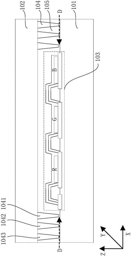
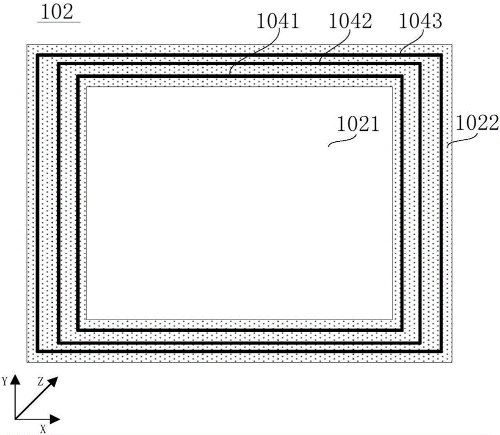
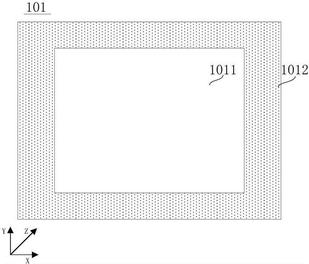
[0047] Figure 4 It is a cross-sectional view of the display panel in the present invention. Figure 5 for Figure 4 Z-direction bottom view of the water-oxygen barrier layer. Figure 6 for Figure 4 Top view of the Z-direction of the middle substrate. Figure 7 It is a schematic diagram of the staggered arrangement of the walls of the first retaining wall and the walls of the second retaining wall in the display panel of...
PUM
 Abstract
Description
Claims
Application Information
 - R&D
- Intellectual Property
- Life Sciences
- Materials
- Tech Scout
- Unparalleled Data Quality
- Higher Quality Content
- 60% Fewer Hallucinations
Browse by: Latest US Patents, China's latest patents, Technical Efficacy Thesaurus, Application Domain, Technology Topic, Popular Technical Reports.
© 2025 PatSnap. All rights reserved.Legal|Privacy policy|Modern Slavery Act Transparency Statement|Sitemap|About US| Contact US: help@patsnap.com


