Array substrate and touch display panel

A touch display panel and array substrate technology, which is applied in the fields of instruments, electrical digital data processing, and data processing input/output processes, etc., can solve problems such as poor panel uniformity, increase panel uniformity, and reduce static electricity residual or static electricity. The effect of the risk of injury

Active Publication Date: 2017-02-01
WUHAN CHINA STAR OPTOELECTRONICS TECH CO LTD
View PDF13 Cites 5 Cited by
  • Summary
  • Abstract
  • Description
  • Claims
  • Application Information

AI Technical Summary

Problems solved by technology

Poor uniformity across the panel due to the presence of bridges between the sensing pads

Method used


Image

  • Array substrate and touch display panel
  • Array substrate and touch display panel
  • Array substrate and touch display panel

Examples


Embodiment Construction

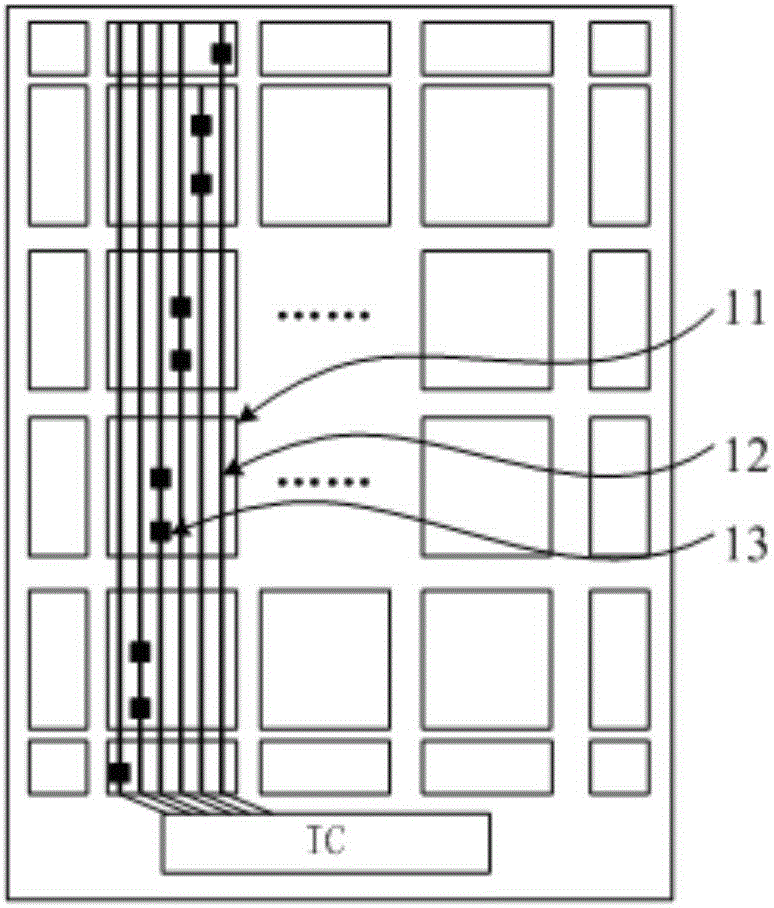
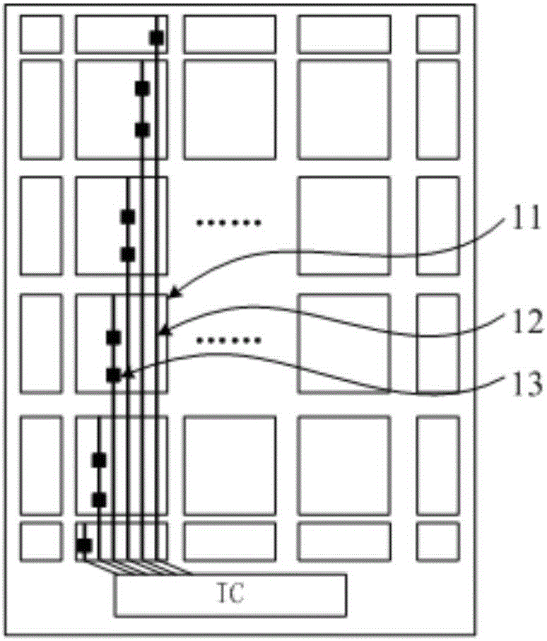
[0016] The array substrate and touch display panel provided by the present invention will be described in detail below with reference to the accompanying drawings.

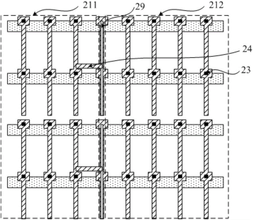
[0017] refer to image 3 , a schematic diagram showing the first embodiment of the array substrate of the present invention. The array substrate includes a plurality of gate lines G1 and a plurality of data lines D1, and a plurality of pixel units P1 surrounded by the gate lines G1 and data lines D1, and the array substrate also includes a common electrode layer and a driving circuit (Fig. not shown).

[0018] The common electrode layer is provided with a zigzag groove 39 (the location is shown by a dotted frame in the figure) to divide the common electrode layer into a plurality of sensing pads (two sensing pads 311, 312 are shown in the figure), The longitudinal slot 391 of the zigzag slot 39 spans 2 pixel units, and the transverse slot 392 of the zigzag slot 39 spans 3 pixel units. Each sensing pad is electr...


PUM


Abstract

The invention discloses an array substrate and a touch display panel. The array substrate comprises a plurality of gate lines, a plurality of data lines, and a plurality of pixel units defined by the gate lines and the data lines; the array substrate further comprises a common electrode layer and a driving circuit; a sawtooth-shaped open slot is formed in the common electrode layer to segment the common electrode layer into a plurality of induction pads; a longitudinal open slot of the sawtooth-shaped open slot is across at least one pixel unit; a transverse open slot of the sawtooth-shaped open slot is across at least three pixel units; each induction pad is electrically connected with the driving circuit through a touch lead wire; and the touch lead wire is connected with the induction pad controlled by the touch lead wire through a via hole in a region, not provided with the sawtooth-shaped open slot, of the common electrode layer. According to the array substrate and the touch display panel, the panel uniformity of an embedded touch display panel can be improved, and in the RGBW embedded touch panel, the influence of the open slot in the common electrode layer on the penetration rate of G color resistance can be reduced.

Description

technical field [0001] The present invention relates to the field of display technology, in particular to an array substrate and a touch display panel that can increase the panel uniformity of an in-cell touch display panel (Incell Touch Panel). Background technique [0002] Touch screen is the main trend of small and medium-sized panels. According to the relative positional relationship among glass panels, touch panels and display panels, touch display devices can be divided into in-cell, on-cell and plug-in types. There are three types. Among them, the embedded touch screen has become an important development direction of touch technology due to its advantages of high integration, thin profile and superior performance. According to the capacitance detection method, the embedded touch screen can be divided into two types: self-capacitance and mutual capacitance. Sensitivity and difference (Differ value) are two important parameters to measure the quality of touch screen. ...

Claims


Application Information

Patent Timeline
IPC IPC(8): G06F3/041G06F3/044
CPCG06F3/0412G06F3/044
Inventor 张春倩王超
Owner WUHAN CHINA STAR OPTOELECTRONICS TECH CO LTD
Why Eureka
Try Eureka