Flexible oled substrate structure and design method

A flexible substrate and substrate technology, which is applied in the directions of organic semiconductor devices, electric solid-state devices, semiconductor devices, etc., can solve the problem of difficult to meet the bending design of flexible OLED substrates, and achieves improved rollability, reduced bending radius, and increased rollability. effect of times

Active Publication Date: 2019-03-12
WUHAN CHINA STAR OPTOELECTRONICS TECH CO LTD
View PDF4 Cites 0 Cited by
  • Summary
  • Abstract
  • Description
  • Claims
  • Application Information

AI Technical Summary

Problems solved by technology

Such a design is difficult to meet the bending design of flexible OLED substrates, so it is urgent to improve

Method used


Image

  • Flexible oled substrate structure and design method
  • Flexible oled substrate structure and design method
  • Flexible oled substrate structure and design method

Examples


Embodiment Construction

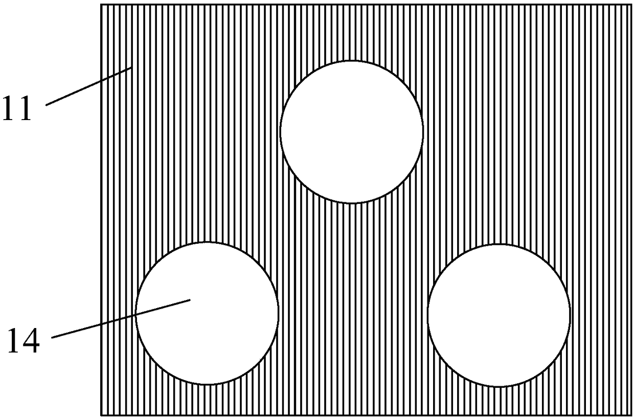
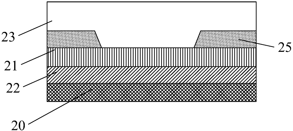
[0029] see figure 1 and figure 2 , figure 1 It is a schematic cross-sectional view of the first preferred embodiment of the flexible OLED substrate structure of the present invention, figure 2 for figure 1 A schematic top view of the first inorganic layer in . The flexible OLED substrate structure mainly includes a flexible substrate 10, a first inorganic layer 11, a second inorganic layer 12, and an organic layer 13. The second inorganic layer 12 is disposed on the flexible substrate 10, and the first inorganic layer 11 is disposed on the flexible substrate. On the second inorganic layer 12 , the organic layer 13 is disposed on the first inorganic layer 11 . The flexible substrate 10 may be a polyimide (PI) substrate. A plurality of via holes 14 are provided on the first inorganic layer 11 where conduction is required to conduct conduction and adjust the pattern density of the inorganic layer. In this embodiment, the via holes 14 are circular, and the ratio of the hol...


PUM


Abstract

The invention relates to a flexible OLED substrate structure and design method. The flexible OLED substrate structure includes a first inorganic layer that requires conduction, and a plurality of via holes are provided on the first inorganic layer where conduction is required to conduct conduction and adjust the pattern density of the inorganic layer. The design method of the flexible OLED substrate structure at least includes: 1. Designing multiple via holes on the inorganic layer where there is a need for conduction; 2. Using a mesh design for the metal layer power supply wiring; 3. Perpendicular to the bending axis Or the signal routing of the winding shaft adopts a serpentine design. The flexible OLED substrate structure and design method of the present invention can increase the foldable times of the flexible OLED, reduce the bending radius, and improve the bendable performance; increase the curlable times of the flexible OLED, reduce the curling radius, and improve the rollable performance.

Description

technical field [0001] The invention relates to the field of active displays, in particular to a flexible OLED substrate structure and design method. Background technique [0002] OLED is a display technology with great development prospects. It not only has excellent display performance, but also has the characteristics of self-illumination, simple structure, ultra-thin, fast response, wide viewing angle, low power consumption and flexible display. Known as the "dream display", it has been favored by major display manufacturers and has become the main force of the third-generation display devices in the field of display technology. OLED displays generally include: a substrate, an anode on the substrate, an organic light-emitting layer on the anode, an electron transport layer on the organic light-emitting layer, and a cathode on the electron transport layer. The materials mainly include Inorganic layer, organic layer and metal layer, etc. [0003] With the development of ...

Claims


Application Information

Patent Timeline
Patent Type & Authority Patents(China)
IPC IPC(8): H01L51/00H01L51/52
CPCH10K77/111H10K50/80H10K2102/311Y02E10/549
Inventor 李鹏
Owner WUHAN CHINA STAR OPTOELECTRONICS TECH CO LTD
Why Eureka
Try Eureka