A Microstrip Double Layer Antenna

A microstrip and antenna technology, applied in the field of microstrip double-layer antennas, can solve the problem of increasingly high requirements, and achieve the effect of good antenna performance and gain

Active Publication Date: 2019-01-04
佛山市佳昇通讯设备有限公司
View PDF5 Cites 0 Cited by
  • Summary
  • Abstract
  • Description
  • Claims
  • Application Information

AI Technical Summary

Problems solved by technology

The antenna structure with resonance characteristics is called antenna antenna, and the antenna structure directly excited by high-frequency current is called active antenna, otherwise it is called passive antenna; in the existing antenna, the antenna is adjusted according to the needs of actual use During design, in order to make the resonant frequency point of the antenna meet the setting requirements, the input impedance of the antenna needs to be adjusted. The adjusted antenna and the ordinary antenna still cannot meet the requirements of the current communication standard. The current communication standard is getting higher and higher. The requirements for antennas are getting higher and higher, and the gain, directivity, and front-to-back ratio of current antennas all need breakthroughs.

Method used


Image

  • A Microstrip Double Layer Antenna
  • A Microstrip Double Layer Antenna
  • A Microstrip Double Layer Antenna

Examples


Embodiment Construction

[0027] The present invention will be described in further detail below in conjunction with the accompanying drawings and specific embodiments, and the implementation scope of the present invention is not limited thereto.

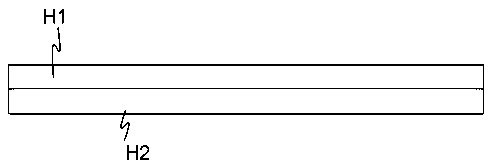
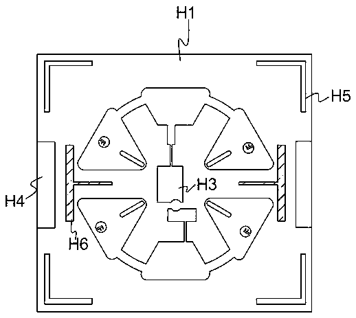
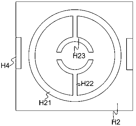
[0028] Such as Figure 1 to Figure 7 As shown, a microstrip double-layer antenna described in this embodiment includes a first PCB board H1 and a second PCB board H2 superimposed together; the top surface of the first PCB board H1 is provided with a first microstrip unit, the first microstrip unit includes two microstrip vibration sets with the same shape and symmetrically arranged; the second microstrip unit is provided on the top surface of the second PCB board H2; the first PCB board H1 and the second PCB board When H2 is superimposed, the second microstrip unit is located on the top surface of the second PCB board H2 and the bottom surface of the first PCB; a kind of microstrip double-layer antenna described in this embodiment, each microstrip vibration ...


PUM


Abstract

Disclosed is a microstrip dual-layer antenna, comprising a first PCB and a second PCB stacked together. A top surface of the first PCB is provided with a first microstrip unit, the first microstrip unit comprising two symmetrically arranged microstrip vibration sets having the same shape. A top surface of the second PCB is provided with a second microstrip unit. When the first PCB and the second PCB are stacked, the second microstrip unit is located on the top surface of the second PCB and a bottom surface of the first PCB. Via an excellent dual-layer structural design and continuous testing and parameter adjustment, the present invention achieves excellent antenna performance and gain with good front-to-back ratio characteristics. The antenna has the features of a low profile, a wide band and a high gain. The 10dB impedance bandwidth of the antenna is 28.4%, and the average gain of a single antenna is 8.2dBi.

Description

technical field [0001] The invention relates to a microstrip double-layer antenna. Background technique [0002] An antenna is a device that converts high-frequency current into radio waves and transmits them into space, and at the same time collects space radio waves and generates high-frequency currents. The antenna can be regarded as a tuned circuit composed of capacitance and inductance; at certain frequency points, the capacitance and inductance of the tuned circuit will cancel each other out, and the circuit will show pure resistance. This phenomenon is called resonance, and the resonance phenomenon corresponds to The working frequency point is the resonant frequency point, and the energy at the resonant frequency point of the antenna has the strongest radiation characteristics. The antenna structure with resonance characteristics is called antenna antenna, and the antenna structure directly excited by high-frequency current is called active antenna, otherwise it is c...

Claims


Application Information

Patent Timeline
Patent Type & Authority Patents(China)
IPC IPC(8): H01Q1/38H01Q1/52H01Q1/50
CPCH01Q1/38
Inventor 覃梅花
Owner 佛山市佳昇通讯设备有限公司
Why Eureka
Try Eureka