
Fingerprint identification module and making method thereof, and fingerprint identification display device

A fingerprint identification module and display device technology, which is applied in the directions of acquiring/arranging fingerprints/palmprints, character and pattern recognition, and printing image collection, etc., which can solve the problems of the area occupied by photodiodes such as the influence of connection holes, and achieve the goal of occupying an area of The effect of maximizing, increasing the photocurrent, and improving the detection accuracy

Active Publication Date: 2016-11-09
BOE TECH GRP CO LTD
View PDF5 Cites 53 Cited by
  • Summary
  • Abstract
  • Description
  • Claims
  • Application Information

AI Technical Summary

Problems solved by technology

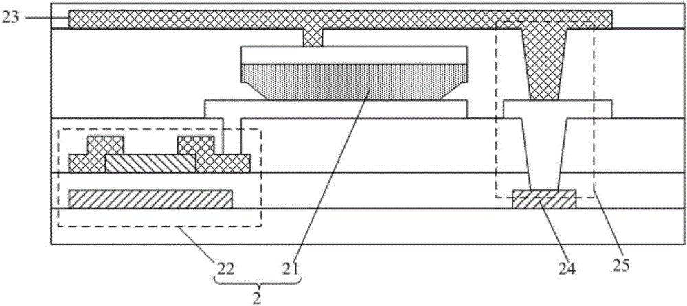
[0004] In view of this, an embodiment of the present invention provides a fingerprint recognition module, its manufacturing method and a fingerprint recognition display device to solve the problem that the area occupied by the photodiode in the existing fingerprint recognition display device is affected by the connection hole

Method used


Image

  • Fingerprint identification module and making method thereof, and fingerprint identification display device
  • Fingerprint identification module and making method thereof, and fingerprint identification display device
  • Fingerprint identification module and making method thereof, and fingerprint identification display device

Examples


Embodiment Construction

[0031] The specific implementations of the fingerprint identification module provided by the embodiments of the present invention, its manufacturing method and the fingerprint identification display device will be described in detail below with reference to the accompanying drawings.

[0032] The shapes and sizes of the components in the drawings do not reflect the true proportions of the fingerprint identification display panel, but are only intended to schematically illustrate the contents of the present invention.

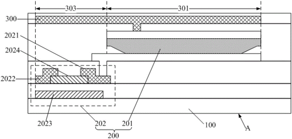
[0033] A kind of fingerprint recognition module that the embodiment of the present invention provides, such as image 3 As shown, it includes: a base substrate 100, a plurality of light-sensitive sensing units 200 arranged in an array arranged on the base substrate 100, and a light-shielding layer 300 disposed on the light-sensitive sensing units 200; wherein, the base substrate 100 is away from The surface on one side of the photosensitive unit 200 is the finge...


PUM


Abstract

The invention discloses a fingerprint identification module and a fingerprint identification display device. A shading layer arranged on photosensitive induction units in the fingerprint recognition module comprises first shading parts arranged above photosensitive diodes of the photosensitive induction units, and fixed potential signal lines, wherein each first shading part is electrically connected with one electrode end of the photosensitive diode below, and each first shading part is connected with the corresponding fixed potential signal line. As the fixed potential signal lines are moved to above the photosensitive diodes and the shading layer is used directly to form the fixed potential signal lines, a space-occupying connecting hole is avoided, the area taken up by the photosensitive diodes is maximized, the photocurrent produced by the photosensitive diodes during fingerprint detection is increased, and the accuracy of fingerprint detection is improved.

Description

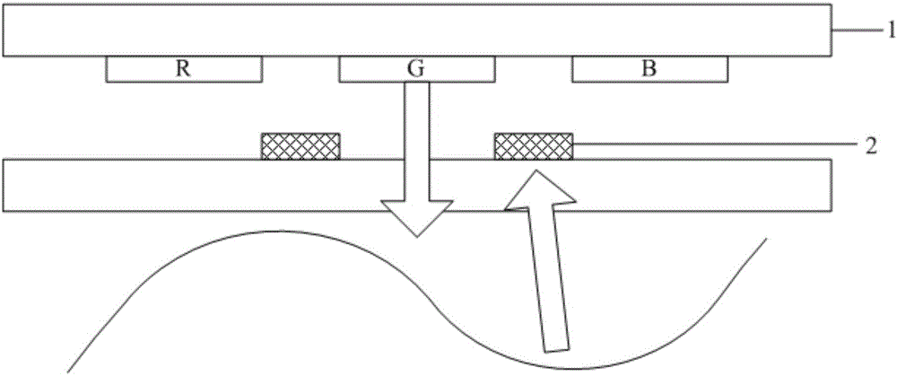
technical field [0001] The invention relates to the field of touch technology, in particular to a fingerprint recognition module, a manufacturing method thereof and a fingerprint recognition display device. Background technique [0002] With the rapid development of display technology, display panels with a fingerprint recognition function have gradually spread in people's lives. At present, in the display device, the photosensitive characteristics such as PIN junction can be used to realize the function of fingerprint identification, and in order not to affect the normal display effect of the display panel 1, that is, not to affect the aperture ratio of the display panel 1, as figure 1 As shown, the photosensitive unit 2 is generally arranged at a position corresponding to the gap between the light emitting regions R, B and G in the display panel 1, that is, the photosensitive unit 2 is arranged at a position corresponding to the non-display region. The photosensitive unit...

Claims


Application Information

Patent Timeline
IPC IPC(8): G06K9/00G06F3/042G06F3/041
CPCG06F3/0412G06F3/0421G06F2203/04109G06V40/1318
Inventor 李昌峰董学吕敬王海生刘英明丁小梁王鹏鹏
Owner BOE TECH GRP CO LTD
Learn More