
Device for growing large-diameter silicon carbide crystal by PVT method

A silicon carbide single crystal and growth device technology, applied in the directions of single crystal growth, single crystal growth, crystal growth, etc., can solve the problems of excessive temperature gradient, fast heating speed, difficult precise control and stable output, etc. The effect of reducing the difficulty of processing, improving the accuracy and easy processing

Active Publication Date: 2016-10-26
SICC CO LTD
View PDF7 Cites 12 Cited by
  • Summary
  • Abstract
  • Description
  • Claims
  • Application Information

AI Technical Summary

Problems solved by technology

[0004] The advantage of the induction heating device is that the heating speed is fast and the efficiency is high, but its disadvantages are also obvious.
Due to the skin effect of induction heating, the heating area is only located on the surface of the growth chamber, and the heating is not uniform enough; when the size of the growth chamber continues to expand, due to the long distance between the heating area and the center of the growth chamber, an excessive radial temperature gradient will be generated
Moreover, the magnetic field of induction heating is greatly affected by factors such as power fluctuations and coil installation accuracy, and it is difficult to achieve precise control and stable output.
In addition, induction heating growth devices generally use double-layer quartz tubes as vacuum chambers, but it is difficult to manufacture large-diameter quartz tubes, so it is difficult to manufacture large-diameter silicon carbide equipment in the prior art
Due to the more precise control of the axial and radial temperature gradients in the growth chamber required during the growth of large-diameter silicon carbide single crystals, the induction heating device is basically unable to meet the demand at this time.

Method used


Image

  • Device for growing large-diameter silicon carbide crystal by PVT method

Examples


Embodiment Construction

[0016] The present invention will be further described below through specific embodiments in conjunction with the accompanying drawings.

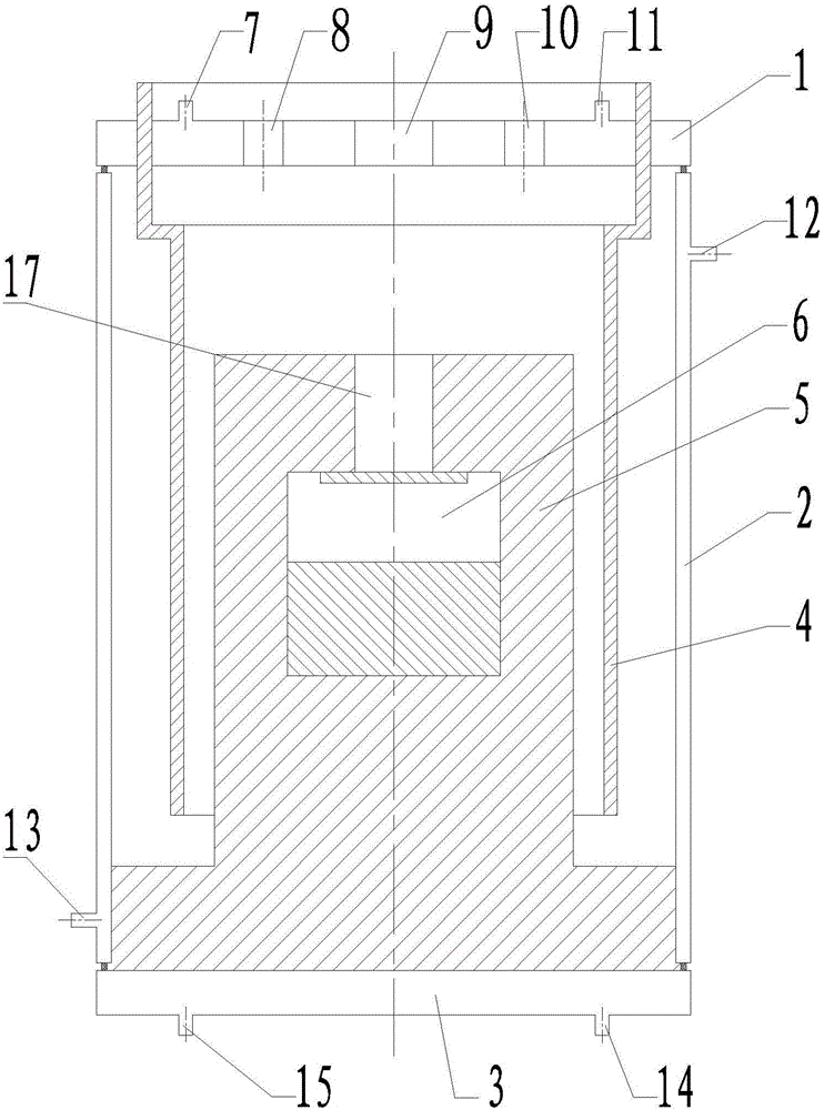
[0017] Such as figure 1 As shown, a large-diameter silicon carbide single crystal growth device by PVT method includes a vacuum chamber, a growth chamber 6, a heater 4, and a thermal insulation material 5, and the growth chamber 6, heater 4, and thermal insulation material 5 are all located in Inside the vacuum chamber. The vacuum cavity is mainly composed of an upper cover 1, a side wall 2, and a lower cover 3, wherein the side wall 2 is a cylindrical structure, the upper cover 1 is sealed and arranged on the upper end of the side wall 2, and the connection between the upper cover 1 and the side wall 2 The sealing ring 16 seals between the upper end surfaces, the lower cover 2 is sealed at the lower end of the side wall 2 , and the sealing ring 16 seals between the lower cover 2 and the lower end surface of the side wall 2 . The growth c...


PUM


Abstract

The invention discloses a device for growing large-diameter silicon carbide crystal by a PVT method, comprising a vacuum cavity as well as a growth chamber and a heater which are arranged in the vacuum cavity, wherein the vacuum cavity is mainly composed of an upper cover, side walls and a lower cover which are hermetically connected sequentially and is characterized in that the upper cover, side walls and lower cover of the vacuum cavity are made of stainless steel and are of a hollow structure, and each of the upper cover, side walls and lower cover is respectively provided with a cooling water inlet and a cooling water return port; the outside of the growth chamber is coated with a thermal insulation material; the heater is of a cylindrical structure and is positioned outside the thermal insulation material; the heater and the growth chamber are coaxially arranged; the heater is a resistance heater; and the vacuum cavity is provided with an extraction opening connected with a vacuum system and an air inlet connected with protective gas. According to the device disclosed by the invention, the resistance heater is used for realizing uniform heating, so that the accuracy of temperature control can be increased; and the device is easy to process, and the size of a temperature field is not limited, so that the device is especially suitable for growth of large-size silicon carbide single crystal.

Description

technical field [0001] The invention relates to a silicon carbide single crystal growth device, in particular to a large-diameter silicon carbide single crystal growth device by PVT method, belonging to the technical field of silicon carbide crystal production equipment. Background technique [0002] Silicon carbide (SiC) is a third-generation wide-bandgap semiconductor material with properties such as wide bandgap, high thermal conductivity, high electron saturation migration rate, and high breakdown electric field. It is comparable to the first-generation semiconductor materials represented by silicon and GaAs Compared with the second-generation semiconductor materials represented by GaN, it has obvious advantages, and it has a lattice structure similar to GaN, so it is considered to be an ideal semiconductor material for manufacturing optoelectronic devices, high-frequency high-power devices, high-temperature electronic devices, etc. . It is widely used in white light li...

Claims


Application Information

Patent Timeline
IPC IPC(8): C30B29/36C30B23/00
CPCC30B23/00C30B29/36
Inventor 于国建宗艳民宋生梁庆瑞
Owner SICC CO LTD
Learn More