
Display device and driving method thereof

A technology of a display device and a driving method, which can be applied to static indicators, instruments, etc., can solve problems such as signal crosstalk, and achieve the effect of reducing parasitic resistance and improving signal crosstalk.

Active Publication Date: 2016-03-02
TCL CHINA STAR OPTOELECTRONICS TECH CO LTD
View PDF6 Cites 11 Cited by
  • Summary
  • Abstract
  • Description
  • Claims
  • Application Information

AI Technical Summary

Problems solved by technology

[0006] The purpose of the present invention is to provide a driving method suitable for a large-size display device, which can reduce the influence of the delay effect caused by the parasitic resistance and capacitance of the scanning line, thereby improving the problem of signal crosstalk

Method used


Image

  • Display device and driving method thereof
  • Display device and driving method thereof
  • Display device and driving method thereof

Examples


Embodiment Construction

[0024] The following descriptions of the various embodiments refer to the accompanying drawings to illustrate specific embodiments in which the present invention can be practiced. The same reference numerals in the embodiments indicate the same or similar components, and the illustrated embodiments are used to illustrate and understand the present invention, but not to limit the present invention.

[0025] Please refer to figure 2 The liquid crystal display device 200 of the present invention includes a plurality of data lines D1-Dkn (n is a positive integer) for transmitting image data voltages, and a plurality of scanning lines G1-Gm (m is a positive integer) for transmitting scanning signals. A scan line and a plurality of data lines are arranged alternately to define each pixel unit 202 , a scan driving circuit 206 , a data driving circuit 208 , and a timing delay control unit 250 . The scanning driving circuit 206 is used for generating a plurality of scanning signals G...


PUM


Abstract

The present invention discloses a driving method of a display device. A plurality of pixel units on each scanning line are divided into a plurality of blocks for scanning and driving, a plurality of interval times are inserted into the scanning period of each scanning line to separate rising edges and falling edges of scanning signals of adjacent blocks, and the thin film transistor of the final pixel unit in each block is able to have fully time to complete charge and switch off with no need for regulation and changing of the duty cycle of the scanning signals. According to the invention, the influence of a delayed effect caused by a parasitic resistance and a parasitic capacitance on a scanning line is effectively reduced, and therefore the problem of signal crosstalk may be improved.

Description

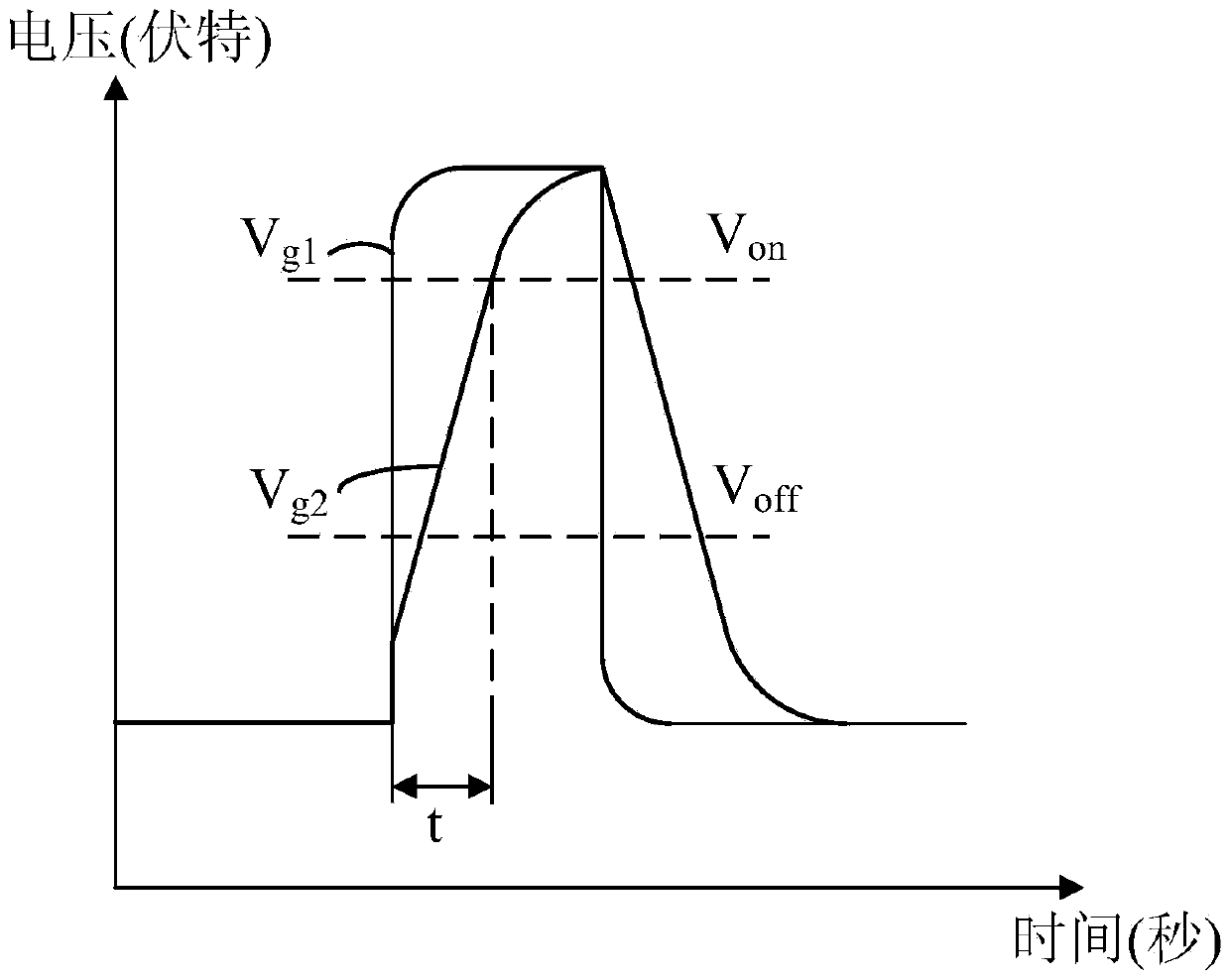
technical field [0001] The present invention relates to the field of display technology, in particular to a display device and a driving method thereof. Background technique [0002] Display devices such as Thin Film Transistor Liquid Crystal Display (TFT-LCD) and Active Matrix Organic Light Emitting Diode (AMOLED) display devices charge pixels by scanning. However, the display device has parasitic resistance and parasitic capacitance in the scanning lines on an active component substrate, which causes RCdelay. Due to the delay effect caused by the parasitic resistance and capacitance of the scanning line, the waveform of the scanning signal changes. [0003] figure 1 It is a scanning signal waveform diagram of a scanning line of a conventional display device. Among them, Von represents the turn-on voltage of the thin film transistor of each pixel unit (subpixel in color display), Voff represents the turn-off voltage of the thin film transistor of each pixel unit, and Vg1...

Claims


Application Information

Patent Timeline
Patent Type & Authority Applications(China)
IPC IPC(8): G09G3/36
Inventor 徐向阳
Owner TCL CHINA STAR OPTOELECTRONICS TECH CO LTD
Learn More