Screen, screen manufacturing method and mobile electronic product
A screen and fixing technology, applied in the field of electronics, can solve the problems of easy cracking and damage of the screen, and achieve the effects of not easy to crack and damage, simple process, and improved reliability.
- Summary
- Abstract
- Description
- Claims
- Application Information
AI Technical Summary
Problems solved by technology
Method used
Image
Examples
Embodiment 1
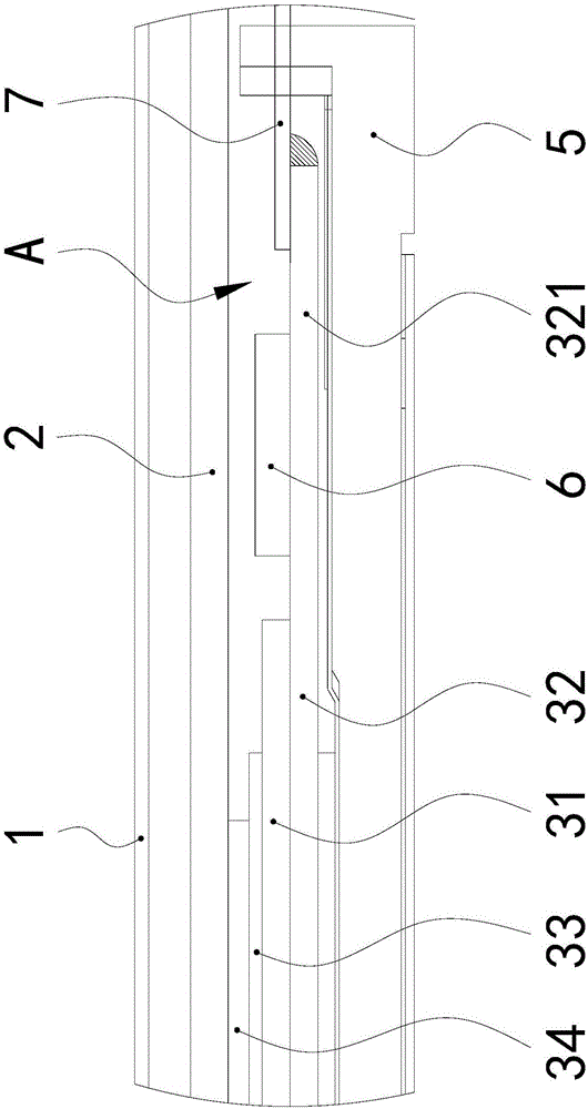
[0023] refer to image 3 , Figure 4 with Figure 5 Embodiment 1 of the present invention provides a screen, including a cover layer 1, a touch-sensitive layer 2 located below the cover layer 1, and a display layer 3 located below the touch-sensitive layer 2, and the display layer 3 includes at least an upper glass A substrate layer 31 and a lower glass substrate layer 32, the touch sensing layer 2 is located above the upper glass substrate layer 31, the lower glass substrate layer 32 is located below the upper glass substrate layer 31, and the lower glass substrate layer 32 has a protrusion A gap A is formed between the protruding portion 321 of the upper glass substrate layer 31 and the touch sensing layer 2 , and a protective pad 4 is disposed in the gap A. Specifically, the screen is an OGS screen or a GFF screen.
[0024] refer to Figure 5 The protective pad 4 includes a lower surface 412 facing the lower glass substrate layer and an upper surface 411 facing the touc...
Embodiment 2
[0035] Embodiment 2 of the present invention provides a mobile and portable electronic product, including a screen, which is the screen described in Embodiment 1. For the specific structure of the screen, refer to Embodiment 1, and will not be described in detail here.
Embodiment 3
[0037] A method of manufacturing a screen, comprising:
[0038] Step 1, setting a cover plate layer, a touch sensing layer and a display layer, the display layer at least includes an upper glass substrate layer and a lower glass substrate layer, the lower glass substrate layer is located below the upper glass substrate layer, and the lower glass substrate layer the layer has a protrusion protruding from the upper glass substrate layer;
[0039] Step 2, setting a protective pad at the protruding part of the lower glass substrate layer;
[0040] Step 3, the cover layer, the touch sensing layer, the protective pad and the display layer are combined together from top to bottom.
[0041] The cover layer and the touch-sensing layer, and the touch-sensing layer and the display layer are respectively bonded together by a layer of optically transparent glue.
[0042] The protection pad is bonded to the protruding part of the lower glass substrate layer, and when the cover layer, the ...
PUM
 Abstract
Description
Claims
Application Information
 - R&D
- Intellectual Property
- Life Sciences
- Materials
- Tech Scout
- Unparalleled Data Quality
- Higher Quality Content
- 60% Fewer Hallucinations
Browse by: Latest US Patents, China's latest patents, Technical Efficacy Thesaurus, Application Domain, Technology Topic, Popular Technical Reports.
© 2025 PatSnap. All rights reserved.Legal|Privacy policy|Modern Slavery Act Transparency Statement|Sitemap|About US| Contact US: help@patsnap.com


