A wafer wet etching cleaning device

A technology of wet etching and cleaning device, applied in the direction of electrical components, semiconductor/solid-state device manufacturing, circuits, etc., can solve the problems of low cleaning efficiency and poor cleaning effect, and achieve simple structure, enhanced corrosion resistance and heat resistance. , to achieve the effect of stability

Active Publication Date: 2017-09-19
THE 45TH RES INST OF CETC
View PDF4 Cites 0 Cited by
  • Summary
  • Abstract
  • Description
  • Claims
  • Application Information

AI Technical Summary

Problems solved by technology

[0005] The invention provides a wafer wet etching cleaning device. The technical problem to be solved is that the cleaning equipment in the prior art needs to clean different corrosion chemical liquids in multiple devices respectively, and the cleaning efficiency is low and the cleaning effect is poor.

Method used


Image

  • A wafer wet etching cleaning device
  • A wafer wet etching cleaning device
  • A wafer wet etching cleaning device

Examples


Embodiment Construction

[0042] The principles and features of the present invention are described below in conjunction with the accompanying drawings, and the examples given are only used to explain the present invention, and are not intended to limit the scope of the present invention.

[0043] The embodiments of the present invention need to solve the problem that the wafer cleaning equipment in the prior art needs to clean different corrosion chemical liquids in multiple devices respectively, and the cleaning efficiency is low.

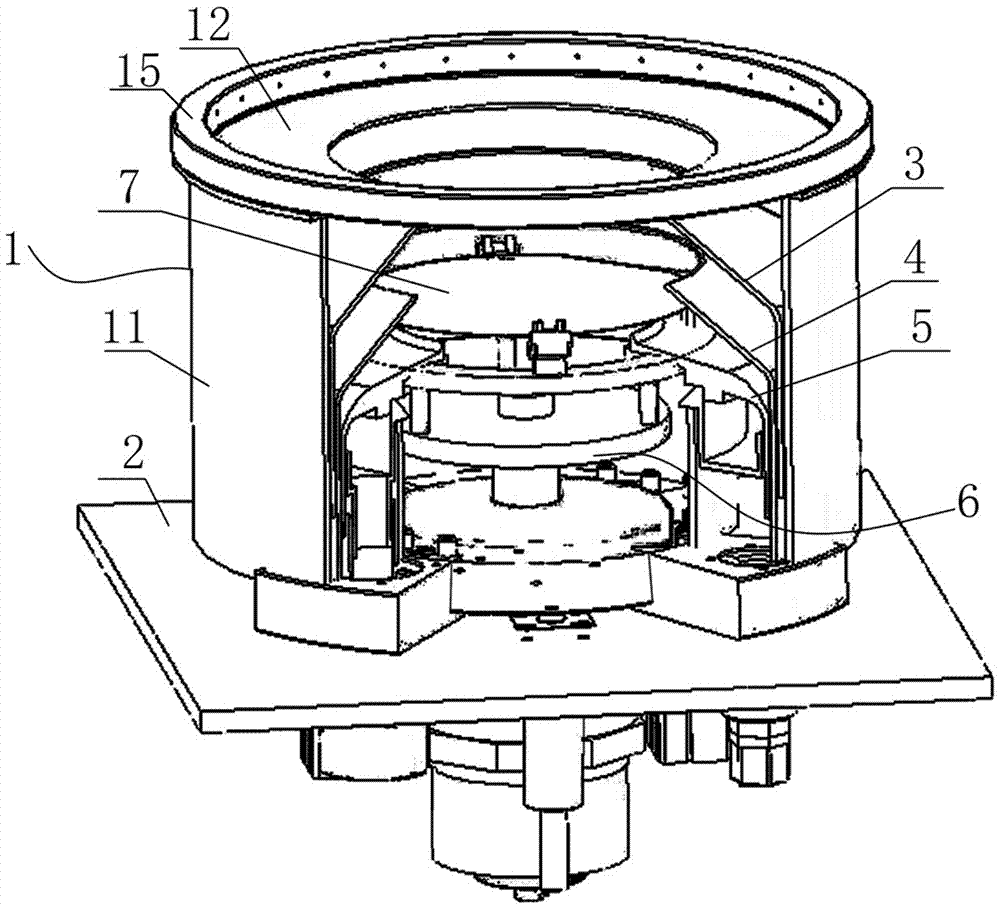
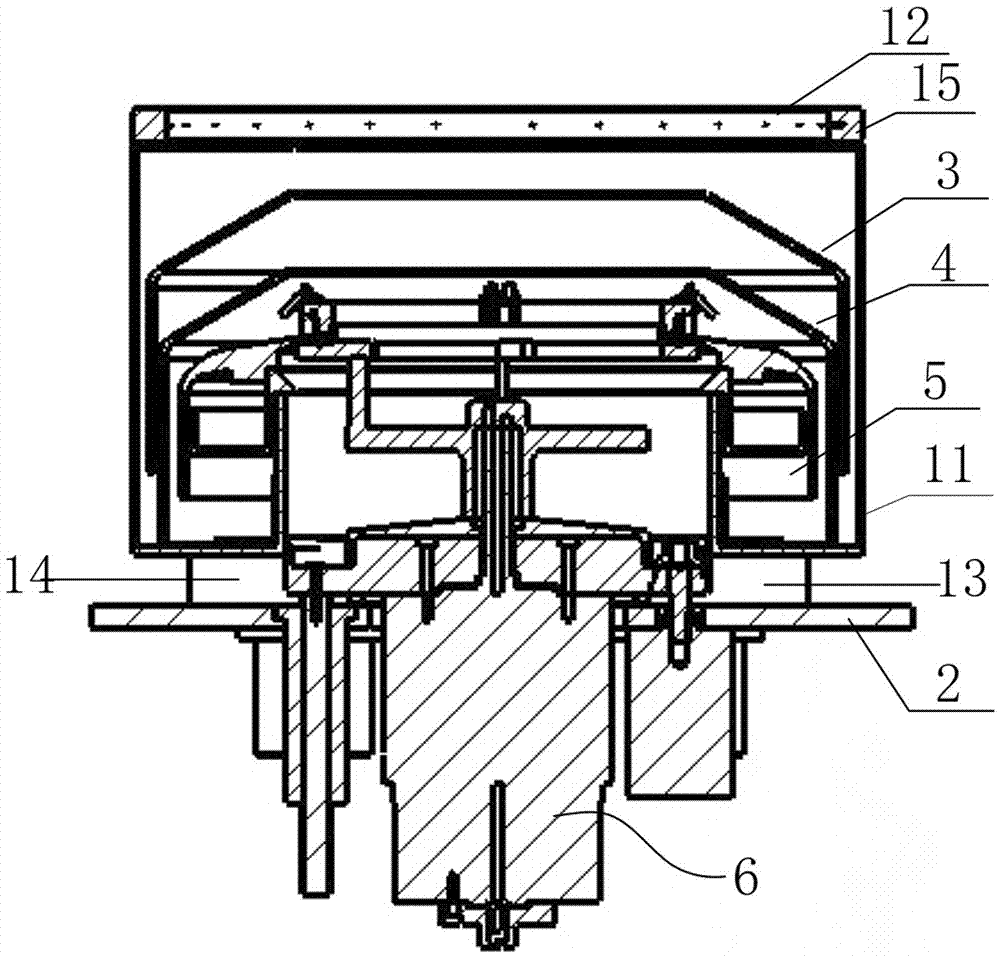
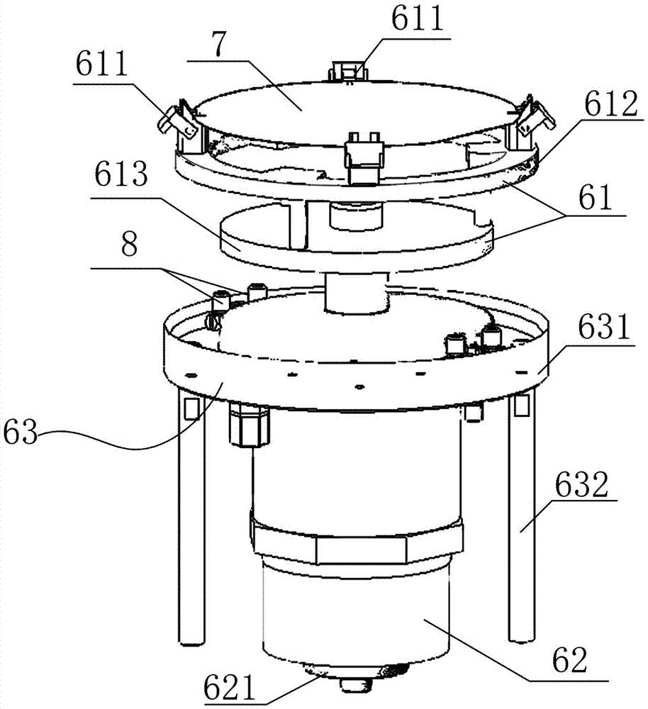
[0044] Such as figure 1 , figure 2 , Figure 6 and Figure 7 As shown, it is a schematic diagram of a wafer wet etching cleaning device provided by an embodiment of the present invention. The wafer wet etching cleaning device includes:

[0045] Housing 1, the housing includes a housing body 11 and a housing upper cover 12, the housing upper cover 12 is arranged on the upper part of the housing 11;

[0046] A work surface 2, the housing 1 is mounted on the work surfac...


PUM


Abstract

The invention relates to a wafer wet etching cleaning device, comprising an outer housing, a working table-board, an N2 gas curtain generating element, a first inner housing, a second inner housing, a third inner housing, a chemical solution spraying element, and a wafer moving part. The outer housing is arranged on the working table-board. The N2 gas curtain generating element is arranged on the upper part of the outer housing. The first inner housing is arranged in the outer housing. The outer housing and the first inner housing form a first working chamber. The second inner housing is arranged in the first inner housing. The second inner housing and the first inner housing form a second working chamber. The third inner housing is arranged in the second inner housing. The third inner housing and the second inner housing form a third working chamber. The chemical solution spraying element is used to spray chemical solution to the surface of wafers. The wafer moving part is used to place wafers in the first working chamber, the second working chamber, and the third working chamber in sequence. Using the cleaning device, wafers complete various chemical liquid etching cleaning function on a station, and cleaning efficiency is improved. In addition, the device realizes independent discharge, recycling and reuse of chemical liquid, and ensures cleanliness requirement.

Description

technical field [0001] The invention belongs to the technical field of wafer cleaning in semiconductor wafer processing, and in particular relates to a wafer wet etching cleaning device. Background technique [0002] During the semiconductor wafer manufacturing process, the wafer needs to go through multiple cleaning steps. Due to the continuous shrinking of the critical dimensions of the device process technology and the introduction of new materials, the surface cleaning treatment in the front-end process (FEOL, font end of line) is more important. The reduction of critical dimensions narrows the cleaning process window, and it is necessary to meet the wafer cleaning efficiency and at the same time achieve the minimum wafer surface loss and particle size requirements. [0003] Wafer wet cleaning is divided into two methods: tank cleaning and single wafer cleaning. Single wafer cleaning can reduce the risk of cross-contamination during cleaning and improve yield. By usin...

Claims


Application Information

Patent Timeline
Patent Type & Authority Patents(China)
IPC IPC(8): H01L21/67
CPCH01L21/67023
Inventor 陈仲武刘玉倩姚立新
Owner THE 45TH RES INST OF CETC
Why Eureka
Try Eureka