a semiconductor device

A technology of semiconductors and devices, which is applied in the direction of instruments, static memory, digital memory information, etc., can solve unsatisfactory problems and achieve the effect of improving performance and writability

Active Publication Date: 2018-11-16
SEMICON MFG INT (SHANGHAI) CORP
View PDF4 Cites 0 Cited by
  • Summary
  • Abstract
  • Description
  • Claims
  • Application Information

AI Technical Summary

Problems solved by technology

However, the improvement effects of these technologies on the write noise margin (WNM) of SRAM cells are often not ideal

Method used


Image

  • a semiconductor device
  • a semiconductor device
  • a semiconductor device

Examples


Embodiment 1

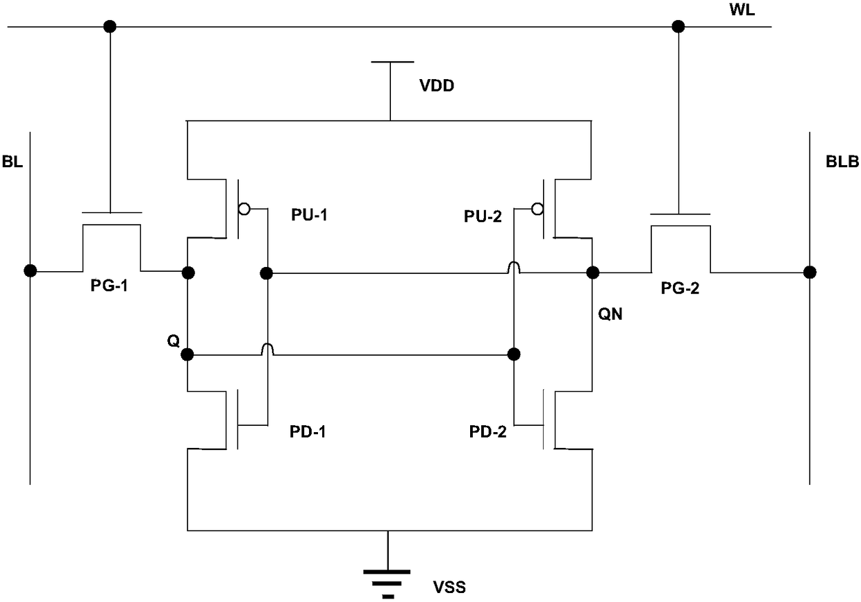
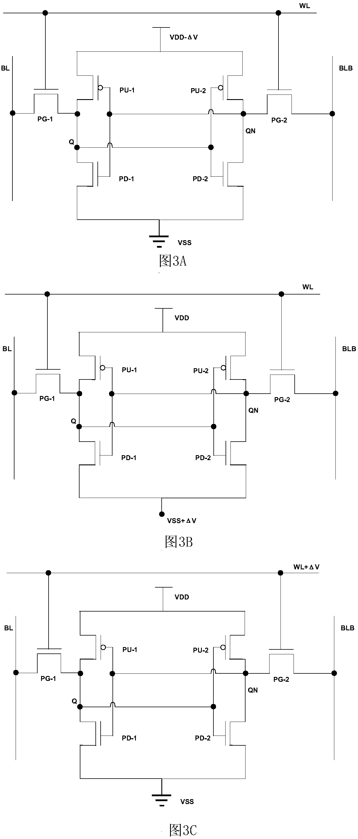
[0037] Below, refer to Figure 4 A semiconductor device according to an embodiment of the present invention will be described. Figure 4 It is a circuit diagram of an SRAM unit in a semiconductor device according to an embodiment of the present invention, wherein, Figure 4 A is the first circuit diagram of the SRAM unit in the semiconductor device of the embodiment of the present invention (embodiment one scheme one); Figure 4 B is the second circuit diagram of the SRAM unit in the semiconductor device of the embodiment of the present invention (the second embodiment of the first embodiment).

[0038] The semiconductor device of the embodiment of the present invention includes a SRAM memory unit, wherein, as shown in Figure 4A and Figure 4 As shown in B, the SRAM unit includes: bit line (BL, BLB), word line (WL), first pull-up transistor (PU-1), second pull-up transistor (PU-2), first pull-down transistor (PD-1), second pull-down transistor (PD-2), pass-gate transistors ...

Embodiment 2

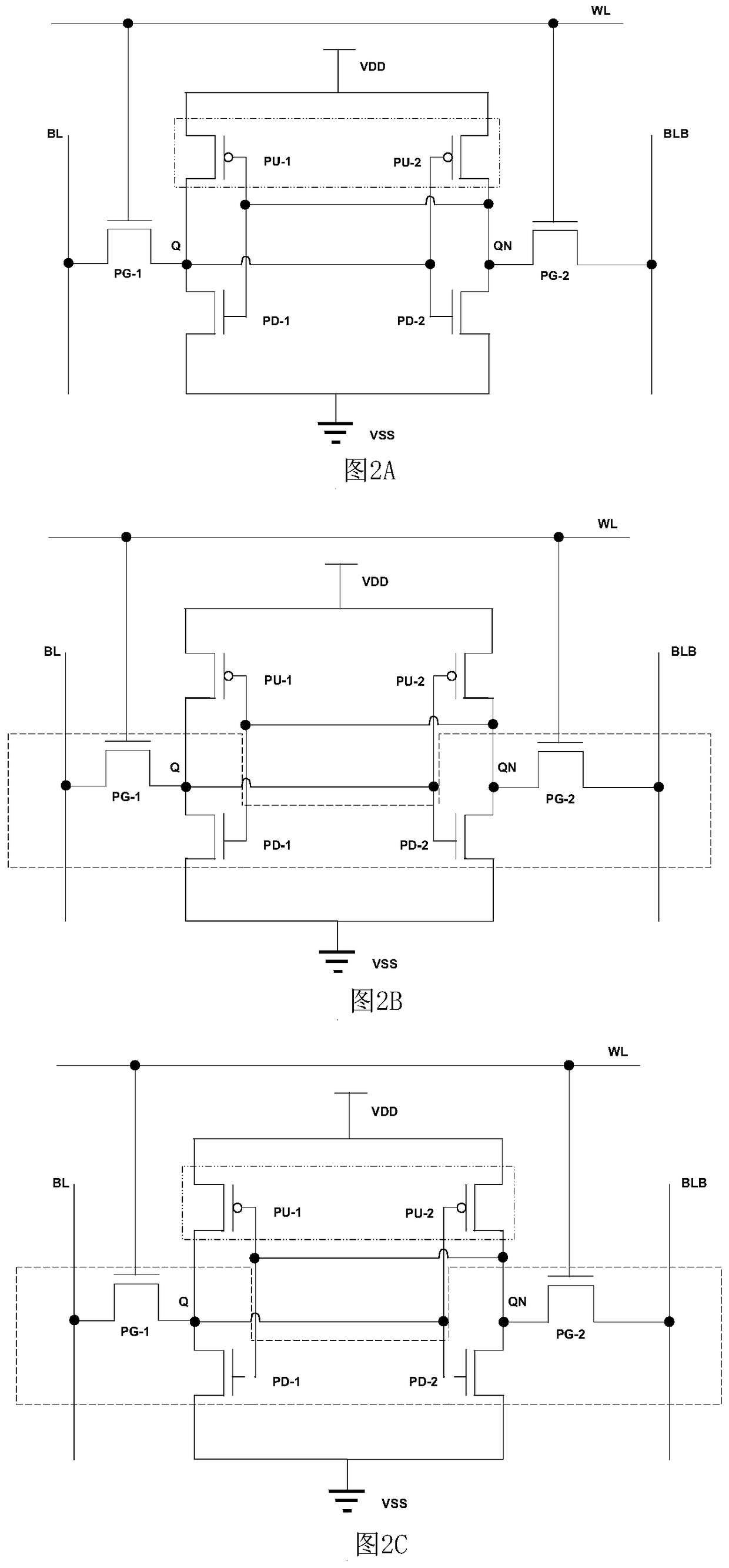
[0046] Below, refer to Figure 5 A semiconductor device according to an embodiment of the present invention will be described. Figure 5 It is a circuit diagram of an SRAM unit in a semiconductor device according to an embodiment of the present invention, wherein, Figure 5 A is the first circuit diagram of the SRAM unit in the semiconductor device of the embodiment of the present invention (embodiment two scheme one); Figure 5 B is a second circuit diagram of the SRAM unit in the semiconductor device of the embodiment of the present invention (Scheme 2 of Embodiment 2).

[0047] The semiconductor device of the embodiment of the present invention includes an SRAM memory unit, wherein, as shown in FIG. 5A and Figure 5 As shown in B, the SRAM unit includes: bit line (BL, BLB), word line (WL), first pull-up transistor (PU-1), second pull-up transistor (PU-2), first pull-down transistor (PD-1), second pull-down transistor (PD-2), pass-gate transistors (PG-1, PG-2). Wherein, ...


PUM


Abstract

The present invention provides a semiconductor device, and relates to the technical field of semiconductors. The semiconductor device comprises an SRAM unit, wherein in the SRAM unit, the electrical connection does not exist between the first pull-up transistor source electrode for connecting the power supply voltage and the second pull-up transistor source electrode for connecting the power supply voltage, or the electrical connection does not exist between the first pull-down transistor source electrode for connecting the power supply negative electrode and the second pull-down transistor source electrode for connecting the power supply negative electrode, such that the writability and the static noise margin of the SRAM unit can be improved by adjusting the respective power supply voltage value or the power supply negative electrode voltage value so as to improve the performance of the semiconductor device.

Description

technical field [0001] The present invention relates to the technical field of semiconductors, in particular to a semiconductor device, in particular to a semiconductor device including an SRAM unit. Background technique [0002] In the field of semiconductor technology, Static Random Access Memory (SRAM) has broad application prospects because of its superior performance. A circuit diagram of a SRAM memory cell in the prior art is as figure 1 As shown, including bit lines (BL, BLB), word lines (WL), pull-up transistors (PU-1, PU-2), pull-down transistors (PD-1, PD-2), pass-gate transistors (PG-1 , PG-2). Wherein, PU-1 and PD-1 form a first inverter, PU-2 and PD-2 form a second inverter, the first inverter and the second inverter are cross-coupled, and the pull-up transistor PU The drains of -1 and PU-2 are connected and connected to a common power supply voltage VDD, and the sources of the pull-down transistors PD-1 and PD-2 are connected and connected to a common power ...

Claims


Application Information

Patent Timeline
Patent Type & Authority Patents(China)
IPC IPC(8): G11C11/413
Inventor 陈金明
Owner SEMICON MFG INT (SHANGHAI) CORP
Why Eureka
Try Eureka