TFT (Thin Film Transistor) array substrate and liquid crystal display panel

An array substrate and substrate technology, which is applied in nonlinear optics, instruments, optics, etc., can solve the problems of reducing the pixel aperture ratio, affecting the quality of the display screen, and increasing the overlapping part of the pixel unit, so as to solve the Beating Mura problem and high aperture ratio. , to avoid the effect of light leakage

Inactive Publication Date: 2015-09-09
NANJING CEC PANDA LCD TECH
View PDF5 Cites 4 Cited by
  • Summary
  • Abstract
  • Description
  • Claims
  • Application Information

AI Technical Summary

Problems solved by technology

However, the extension of the black matrix will lead to an increase in the overlapping portion of the pixel unit between the BM and the TFT substrate, thereby greatly reducing the pixel aperture ratio, thereby affecting the quality of the display screen

Method used


Image

  • TFT (Thin Film Transistor) array substrate and liquid crystal display panel
  • TFT (Thin Film Transistor) array substrate and liquid crystal display panel
  • TFT (Thin Film Transistor) array substrate and liquid crystal display panel

Examples


Embodiment Construction

[0013] Below in conjunction with accompanying drawing and specific embodiment, further illustrate the present invention, should be understood that these embodiments are only for illustrating the present invention and are not intended to limit the scope of the present invention, after having read the present invention, those skilled in the art will understand various aspects of the present invention Modifications in equivalent forms all fall within the scope defined by the appended claims of this application.

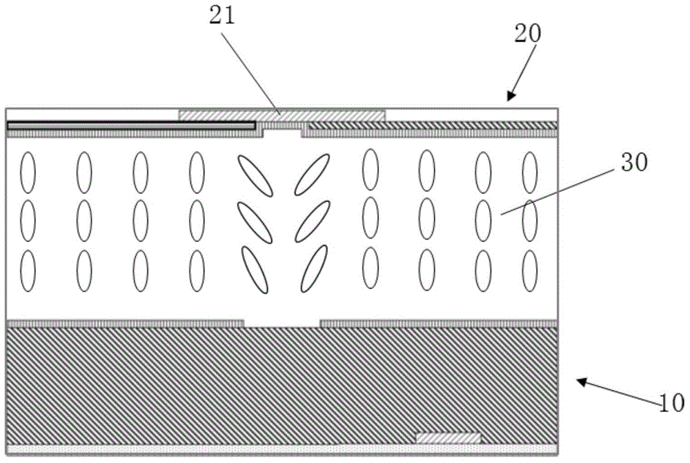
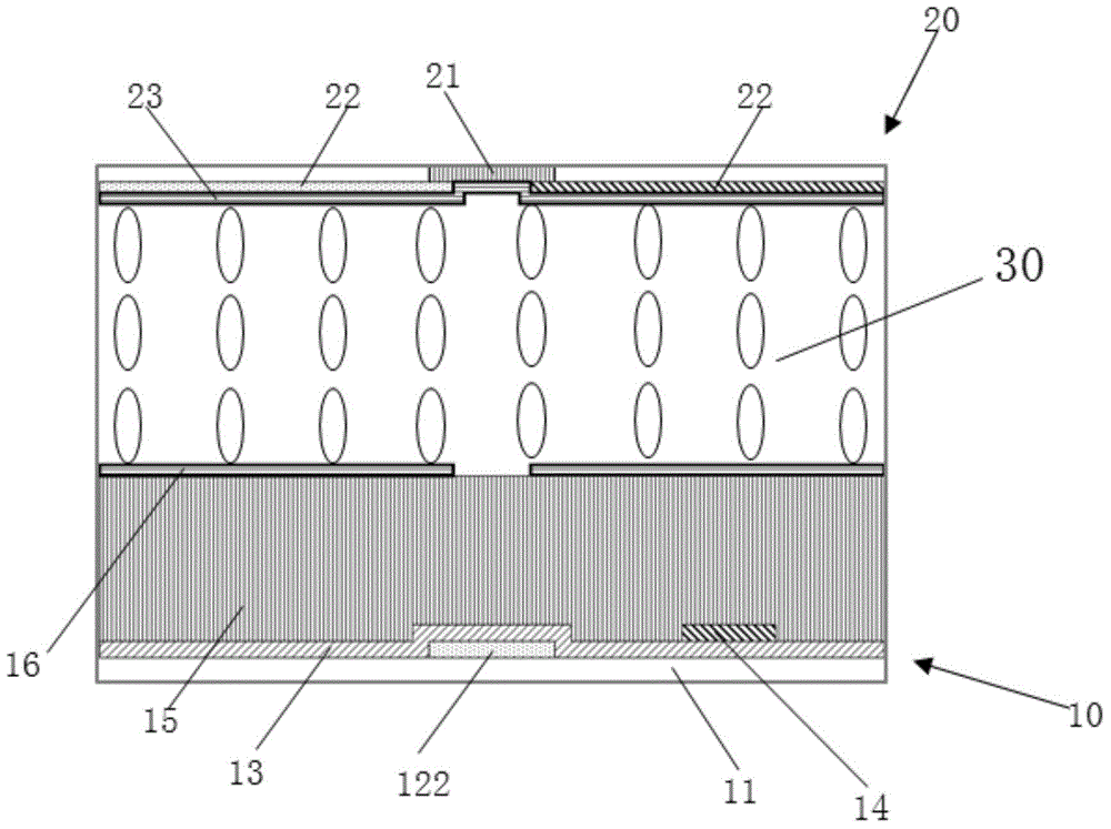
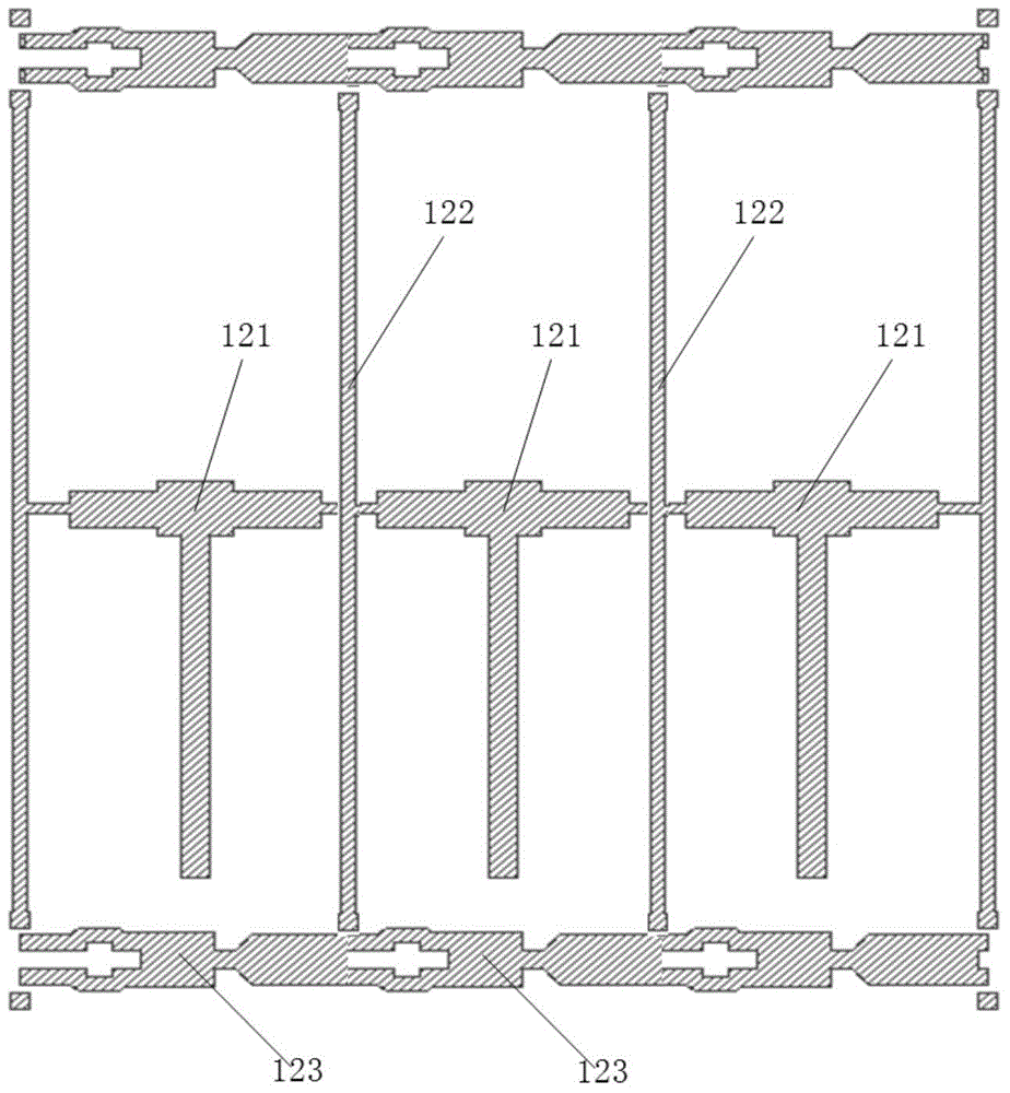
[0014] In order to solve the problems of the prior art, the present invention provides a liquid crystal display panel, such as Figures 2 to 4 As shown, the panel includes: an upper substrate 20 and a lower substrate 10 oppositely arranged, and a liquid crystal layer 30 arranged between the upper substrate and the lower substrate. The lower substrate 10 is a TFT substrate, and the upper substrate 20 is a color filter substrate. The color filter substrate includes a plur...


PUM


Abstract

The invention discloses a TFT (Thin Film Transistor) array substrate. The TFT array substrate comprises a pixel array which is formed on the TFT array substrate; every pixel is provided with a pixel electrode layer and a public electrode layer; every pixel electrode layer is provided with a pixel electrode; every public electrode layer is provided with a first public electrode and a second public electrode, wherein every second public electrode is connected with the corresponding first public electrode; every first public electrode is located in a pixel area; every second public electrode is located between the two corresponding adjacent pixels; the projection of every second public electrode on the corresponding pixel electrode layer and the two adjacent pixel electrodes are partially overlapped; every pixel comprises a data line which is located in the pixel area; the projection of every data line on the corresponding public electrode layer and the corresponding second public electrode are not overlapped. According to the TFT array substrate and a liquid crystal display panel, every second public electrode is arranged between the two corresponding adjacent pixel electrodes so as to ensure that liquid crystal molecules within the electric field line control range of every second public electrode do not deflect freely and accordingly the light leakage is avoided.

Description

technical field [0001] The invention relates to a TFT array substrate and a liquid crystal display panel comprising the TFT array substrate. Background technique [0002] In recent years, flat-panel displays have been favored by people, and the requirements for display quality have been continuously improved. The aperture ratio of liquid crystal displays is one of the important factors affecting the display quality of display devices. A lower aperture ratio not only affects the quality of the screen, but also affects the display quality. power consumption of the device. There are many factors affecting the aperture ratio of a liquid crystal display device, one of which is Beating Mura (squeeze chromatic aberration). When the panel is squeezed, the relative displacement between the color filter substrate (CF) and the TFT substrate will occur, and light leakage will occur at the position that cannot be blocked by the black matrix (BM) of the color filter substrate after dislo...

Claims


Application Information

Patent Timeline
Patent Type & Authority Applications(China)
IPC IPC(8): G02F1/1343G02F1/1362
CPCG02F1/134327G02F1/136286G02F1/1368G02F1/134318
Inventor 周刘飞王鸣昕
Owner NANJING CEC PANDA LCD TECH
Why Eureka
Try Eureka