
A device for preventing wafer back contamination

A wafer and backside technology, applied in the field of devices for preventing contamination of the backside of the wafer, can solve the problems of loss of the protective effect of the backside of the wafer, large impact force, and inability to protect the backside of the wafer well from contamination, etc. the effect of the ability

Active Publication Date: 2018-01-26
BEIJING SEVENSTAR ELECTRONICS CO LTD
View PDF8 Cites 0 Cited by
  • Summary
  • Abstract
  • Description
  • Claims
  • Application Information

AI Technical Summary

Problems solved by technology

This will make the vent hole 2 of the nitrogen cover 1 on the chuck far away from the back of the wafer
At the same time, in the existing chuck structure, the nitrogen gas injected from the nitrogen cover can only ensure that a circle of vertical nitrogen protection layer is formed around the back edge of the wafer. If any pollutants pass through this protection layer, the nitrogen protection layer will protection of the backside of the wafer will be lost
Moreover, during the high-speed rotation of the wafer, after the cleaning liquid is thrown off the wafer surface, it hits the side wall of the cleaning chamber and splashes back to the back of the wafer. The impact force is very strong, and it is easy to cross this vertical nitrogen protective layer and contaminate the back of the wafer.
[0006] Therefore, the current device for preventing contamination on the back of the wafer cannot well protect the back of the wafer from contamination, and a new structural device needs to be designed to solve the problem of contamination on the back of the wafer

Method used


Image

  • A device for preventing wafer back contamination
  • A device for preventing wafer back contamination
  • A device for preventing wafer back contamination

Examples


Embodiment Construction

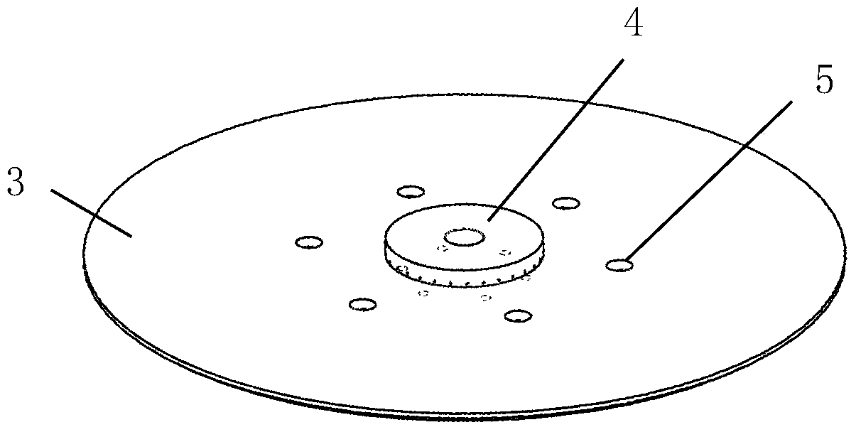
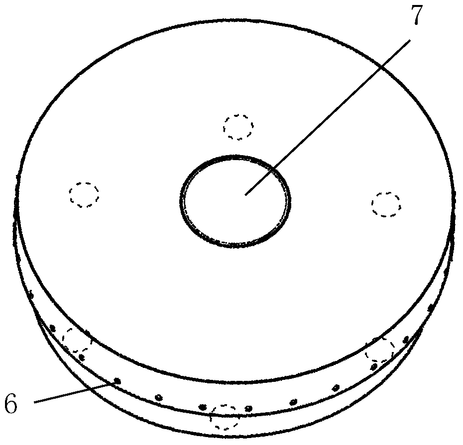
[0025] The specific embodiment of the present invention will be further described in detail below in conjunction with the accompanying drawings.

[0026] It should be noted that, in the following specific embodiments, when describing the embodiments of the present invention in detail, in order to clearly show the structure of the present invention for the convenience of description, the structures in the drawings are not drawn according to the general scale, and are drawn Partial magnification, deformation and simplification are included, therefore, it should be avoided to be interpreted as a limitation of the present invention.

[0027] In the existing device structure for preventing contamination on the back of the wafer, since it is necessary to ensure that the manipulator takes the wafer from the bottom of the wafer, there needs to be a certain height between the clamping part, the chuck and the nitrogen cover to ensure that the manipulator can enter and exit. This places ...


PUM


Abstract

The invention discloses a wafer back surface pollution prevention device which is applied to semiconductor uniwafer cleaning equipment. The wafer back surface pollution prevention device comprises a nitrogen cover which is concentrically arranged at the upper surface of a rotating clamping disc. An air ejection mechanism is convexly arranged at the middle part of the upper surface of the nitrogen cover. Multiple air outlets are evenly arranged around the side surface of the air ejection mechanism. The air outlets are arranged in a manner of facing the edge direction of the back surface of a wafer arranged on the air outlets in a radiation shape at a certain upward tilting angle so that taking and placing of the wafer of a manipulator are not influenced, and a circle of inverted umbrella-shaped air protective layer intersected with the edge of the back surface of the wafer is enabled to be formed by air ejected out of the air outlets. Therefore, the whole back surface of the wafer is ensured to be protected by air, the back splashed cleaning fluid can be effectively blocked and thus secondary pollution to the back surface of the wafer can be avoided.

Description

technical field [0001] The invention relates to the technical field of semiconductor equipment manufacturing, and more particularly, relates to a device for preventing back contamination of wafers used in single-wafer cleaning equipment. Background technique [0002] The current single wafer cleaning equipment mainly achieves the purpose of cleaning by spraying cleaning liquid on the surface of the wafer rotating at high speed. During cleaning, the wafer is held by a plurality of holding members mounted on a circular chuck body, holding the wafer for high-speed rotation. However, if the rotation speed of the wafer is too low, the cleaning solution on the front side of the wafer will soak from the edge of the wafer to the back side of the wafer; and if the rotation speed of the wafer is too high, the cleaning solution on the front side of the wafer will be thrown towards the The side wall of the cleaning chamber collides with the side wall of the cleaning chamber and splashe...

Claims


Application Information

Patent Timeline
Patent Type & Authority Patents(China)
IPC IPC(8): H01L21/67
CPCH01L21/67051
Inventor 刘效岩吴仪赵曾男张豹姬丹丹
Owner BEIJING SEVENSTAR ELECTRONICS CO LTD
Learn More