ROM read data internal clock pulse generation circuit and method

An internal clock and circuit generation technology, applied in read-only memory, information storage, static memory, etc., can solve the problems of ROM reading speed slowdown, ROM power consumption increase, etc., to reduce ROM power consumption and read time, The effect of reducing the payload size

Active Publication Date: 2015-05-20
SHANGHAI HUAHONG GRACE SEMICON MFG CORP
View PDF3 Cites 0 Cited by
  • Summary
  • Abstract
  • Description
  • Claims
  • Application Information

AI Technical Summary

Problems solved by technology

However, in actual use, the Rom Code of many users does not allow the bit line to be fully loaded.
In this case, the too wide internal clock pulse will have a large time margin after successfully reading the data, and these time margins will bring the following two disadvantages: 1) ROM power consumption rises; 2) ROM reading speed slowing down

Method used


Image

  • ROM read data internal clock pulse generation circuit and method
  • ROM read data internal clock pulse generation circuit and method
  • ROM read data internal clock pulse generation circuit and method

Examples


Embodiment Construction

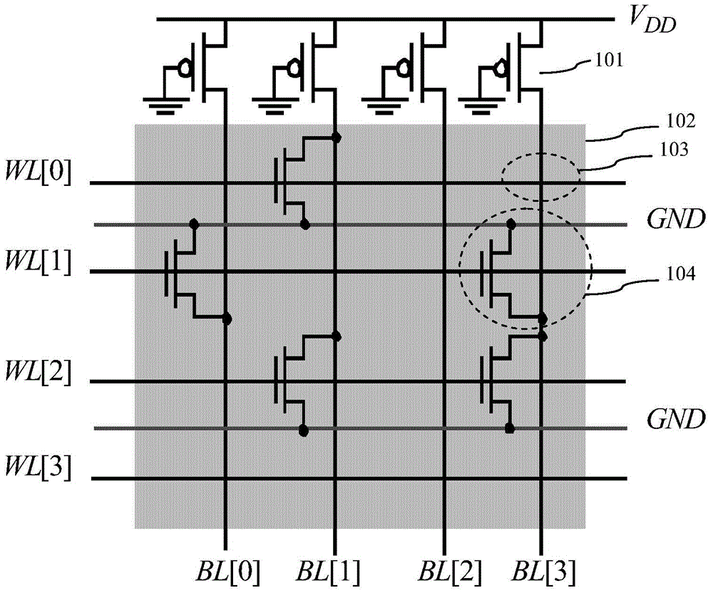
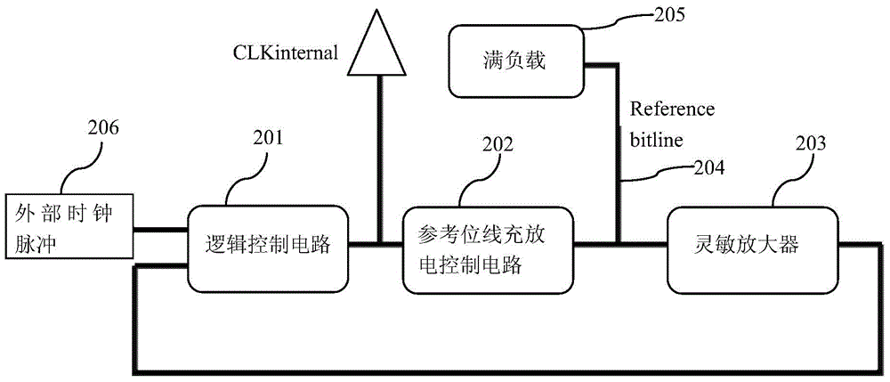
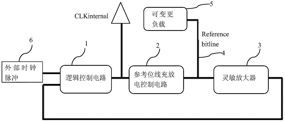
[0031] Such as image 3 What is described is a schematic diagram of the internal clock pulse generating circuit for ROM reading data in the embodiment of the present invention; the internal clock pulse generating circuit for ROM reading data in the embodiment of the present invention includes: logic control circuit 1, reference bit line 4 charge and discharge control circuit 2, and sensitive amplifier circuit 3. The reference bitline is Reference bitline4;

[0032] The load of the reference bit line 4 is a changeable load 5, and the changeable load 5 is adjusted according to the maximum bit line load in the ROM circuit after the ROM data code is written into the ROM circuit.

[0033] The reference bit line 4 charge and discharge control circuit 2 is used to charge and discharge the reference bit line 4 and obtain a charge and discharge time, and the charge and discharge time is determined by the variable load 5.

[0034] The sensitive amplifying circuit 3 and the logic control circui...


PUM


Abstract

The invention discloses an ROM read data internal clock pulse generation circuit. The ROM read data internal clock pulse generation circuit comprises a logic control circuit, a reference bit charging / discharging control circuit, a sensitive amplification circuit and a reference bit, wherein a load of the reference bit is a changeable load; after the changeable load is written into an ROM circuit according to an ROM data code, a maximum bit load in the ROM circuit is adjusted; the reference bit charging / discharging control circuit is used for charging and discharging the reference bit to obtain charging and discharging time of the reference bit; and an internal clock pulse is generated by the sensitive amplification circuit and the logic control circuit, and the pulse width of the internal clock pulse guarantees that accurate reading is realized by sufficient time margin when data on the bit corresponding to the maximum bit load is read. The invention further discloses an ROM read data internal clock pulse generation method. The ROM power consumption and reading time can be reduced.

Description

Technical field [0001] The invention relates to the field of semiconductor integrated circuit manufacturing, in particular to a ROM read data internal clock pulse generation circuit; the invention also relates to a ROM read data internal clock pulse generation method. Background technique [0002] Read-only memory (Read-Only Memory, ROM) is a memory that can only read data. In the wafer manufacturing process, the ROM data code (Code) provided by the customer is usually manufactured in the ROM circuit with a special mask (Mask). The ROM Code here refers to the data that the customer needs to write into the ROM circuit, Code Once written, no changes can be made. [0003] For ROM, general users are more concerned about the following parameters: 1) ROM area; 2) ROM power consumption; 3) ROM reading speed. [0004] When the same ROM is written with different ROM Code, the load on the ROM bit line (Bit Line, BL) will also be different, and the load on the bit line is the code written. T...

Claims


Application Information

Patent Timeline
Patent Type & Authority Applications(China)
IPC IPC(8): G11C17/08
Inventor 潘炯杨光华
Owner SHANGHAI HUAHONG GRACE SEMICON MFG CORP
Why Eureka
Try Eureka