


Quick Research
Generate reliable direction feasibility study reports for your R&D in just a few steps.

Technical Q&A
Discover and master advanced knowledge NOW. Basics, ideas, possibilities, all at once.

Find Solutions
As an expert in R&D theories, this can generate solutions to your technical problems instantly.

Evaluate Feasibility
Analyze your overall solution with one click, know your potential R&D risks in advance.

Monitor Landscape
Get weekly tech updates, stay abreast of the latest tech innovations and key insights.
Power factor improver circuit with function of PFC (power factor correction)
A power factor and circuit technology, applied in the field of switching power supply, can solve the problems of large drop in PF value at full load, ineffective use of electric energy, excessive apparent power, etc., and achieve the effect of improving the ability to correct waveforms
- Summary
- Abstract
- Description
- Claims
- Application Information
AI Technical Summary
Problems solved by technology
Method used
Image

Examples
no. 1 example
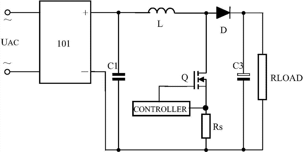
[0024] image 3 A schematic circuit diagram of a PFC power factor boosting circuit according to the first embodiment of the present invention is shown. A PFC power factor boosting circuit 201 is connected between an AC input rectifier circuit 101 and a PFC power circuit 301 .
[0025] The boosting circuit 201 includes a first capacitor, the positive pole of the first capacitor is connected to the positive output terminal of the rectifier circuit, the negative pole of the first capacitor is connected to the negative output terminal of the rectifier circuit; the second capacitor and the first switch are connected, and the positive pole of the second capacitor is connected to the rectifier circuit. The positive output terminal of the circuit is simultaneously connected to the positive pole of the first capacitor, the negative pole of the second capacitor is connected to one end of the first switch, the other end of the first switch is connected to the negative output terminal of t...
no. 2 example
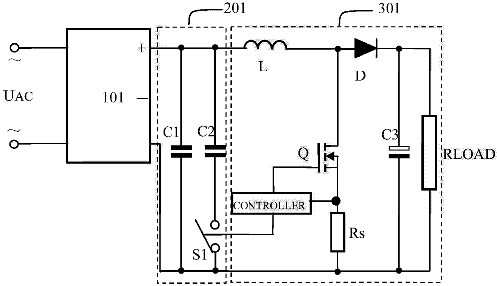
[0038] Figure 5 It shows the schematic circuit diagram of the PFC power factor boosting circuit of the second embodiment, a PFC power factor boosting circuit 201 ′, which is connected between the AC input rectifying circuit 101 and the PFC power circuit 301 .
[0039] The circuit 201' includes a capacitor C1 and a capacitor C2, the positive pole of the capacitor C1 is connected to the positive output terminal of the rectifier circuit, the negative pole of the capacitor C1 is connected to the positive pole of the capacitor C2, and also connected to one end of the switch S1, and the negative pole of the capacitor C2 is connected to the other end of the switch S1 One end is connected to the negative output end of the rectifier circuit.
[0040] The working principle of the circuit 201' for improving the power factor of the PFC circuit under light load conditions is as follows:
[0041] After the circuit is energized for the first time, the input AC power passes through the rect...
no. 3 example
[0049] Such as Figure 6 Shown is the circuit schematic diagram of the power factor boosting circuit of the PFC of the third embodiment of the present invention, a kind of power factor boosting circuit 201 ", differs from the first embodiment in that it also includes a resistor R1, one end of the resistor R1 The capacitor C2 is connected to the positive output end of the rectification circuit, and the other end of the resistor R1 is connected to the negative output end of the rectification circuit through the switch S1.
[0050] Since the resistor R1 is added to the drain branch of the MOS tube, the damage to the MOS tube caused by the high peak current when the switch S1 and the capacitor C2 are directly shorted is avoided, and the MOS tube is protected to a certain extent.
PUM
 Abstract
Description
Claims
Application Information
 - R&D Engineer
- R&D Manager
- IP Professional
- Industry Leading Data Capabilities
- Powerful AI technology
- Patent DNA Extraction
Browse by: Latest US Patents, China's latest patents, Technical Efficacy Thesaurus, Application Domain, Technology Topic, Popular Technical Reports.
© 2024 PatSnap. All rights reserved.Legal|Privacy policy|Modern Slavery Act Transparency Statement|Sitemap|About US| Contact US: help@patsnap.com