Eureka AIR delivers breakthrough ideas for toughest innovation challenges, trusted by R&D personnel around the world.

Use of a semiconducting compound in an organic light emitting device

A compound and application technology, applied in the application field of semiconductor compounds in organic light-emitting devices, can solve problems such as unclear thermal stability, and achieve the effect of high thermal stability

Active Publication Date: 2015-01-28
NOVALED GMBH
View PDF13 Cites 9 Cited by
  • Summary
  • Abstract
  • Description
  • Claims
  • Application Information

AI Technical Summary

Problems solved by technology

Furthermore, given the missing data, it is unclear whether all the compounds proposed confer high thermal stability on devices using them

Method used

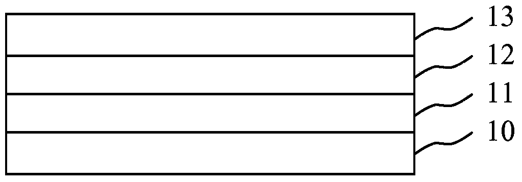
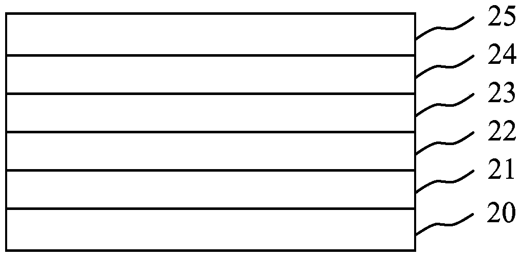

Image

  • Use of a semiconducting compound in an organic light emitting device
  • Use of a semiconducting compound in an organic light emitting device
  • Use of a semiconducting compound in an organic light emitting device

Examples


Embodiment 1

[0206] Bottom blue emitting OLEDs were fabricated on glass substrates coated with patterned ITO (90 nm thickness) with the following layer sequence:

[0207] 1. p-doped N,N'-bis(naphthalene-1-yl)-N,N'-bis(phenyl)-benzidine (a-NPD) (5 mol% of 2,2',2 ″-(cyclopropane-1,2,3-triylidene) tris(2-(p-cyanotetrafluorophenyl)acetonitrile) (PD2) is used as a hole injection and transport layer with a thickness of 130nm;

[0208] 2. Undoped 4,4',4"-tris(carbazol-9-yl)-triphenylamine (TCTA), with a thickness of 10nm;

[0209] 3. Emitter layer with TPBI:Firpic (molar ratio 4:1) with a thickness of 15 nm. TPBI is 1,3,5-tris(1-phenyl-1H-benzimidazol-2-yl)benzene and Firpic is bis(3,5-difluoro-2-(2-pyridyl-(2-carboxy pyridyl) iridium (III);

[0210] 4.20nm TPBI;

[0211] 5.40nm tetrakis(1,3,4,6,7,8-hexahydro-2H-pyrimido[1,2-a]pyrimidinate) ditungsten(II)(W 2 (hpp) 4 ) doped compound C1 (70:30 mol%);

[0212] 6. Cathode of 100nm Al.

[0213] Encapsulate the device with a cover glass layer...

Embodiment 2

[0215] A second OLED was fabricated as described in Example 1, except that compound C2 was used instead of compound C1. at 10mA / cm 2 The voltage at 4.3V and the device reaches 1000cd / m at 4.8V 2 .

Embodiment 3

[0217] A third OLED was fabricated as described in Example 1, except that Compound C3 was used instead of Compound Cl. at 10mA / cm 2 The voltage at 4.0V and the device reaches 1000cd / m at 4.2V 2 .


PUM

PropertyMeasurementUnit
thicknessaaaaaaaaaa
glass transition temperatureaaaaaaaaaa

Abstract

The invention relates to a use of a compound according to formula (1), wherein each of R1, R2, R1, R2 is independently selected from H, C1-C6 alkyl, C1-C6 haloalkyl and C6-C10 aryl or both substituents on the same aromatic ring of the xanthene skeleton are hydrocarbyi groups linked with each other to form together an anelated divalent C2-C10 hydrocarbyi group; X and X' are independently selected from C and N, R5 is H if X is C, R5 is H if X' is C, R5 is lone electron pair if X is N, R5 is lone electron pair if X' is N, and each of R3, R4, R3, R4 is independently selected from H and C6-C10 aryl, with the proviso that neither both R3, R4 nor both R3, R4 are aryl at the same time and if X is C, R3and R4 are not H at the same time, and if X' is C, R3 and R4 are not H at the same time, or both substituents on the same phenyl or pyridyl ring are hydrocarbyi groups linked with each other to form together a divalent C4-C10 hydrocarbyi group representing an anelated, substituted or unsubstituted, six-membered aromatic ring; in an electron transporting layer or in an electron injecting layer comprised in an electronic device.

Description

Background technique [0001] Since Tang et al. disclosed efficient organic light-emitting diodes (OLEDs) in 1987 (C.W.Tang et al., Appl. Technology progresses to high-end commercial displays and lamps. OLEDs contain a series of thin layers essentially made of organic materials between two electrodes. This layer typically has a thickness in the range of 1 nm to 5 μm. This layer is usually formed in vacuum by means of vapor deposition or from solution, for example by means of spin coating or printing. [0002] OLEDs emit light after injecting charge carriers into the light-emitting layer from the cathode side in the form of electrons and from the anode side in the form of holes. Charge carrier injection is achieved based on an applied external voltage, then excitons are formed in the light-emitting region, and these excitons radiatively recombine. At least one electrode is transparent or translucent, in most cases in the form of a transparent oxide, such as indium tin oxide (...

Claims


Application Information

Patent Timeline
Patent Type & Authority Applications(China)
IPC IPC(8): C09K11/06H05B33/14
CPCH05B33/14C09K2211/1088C09K11/06C07D311/96C07D405/14H10K85/626H10K50/11H10K50/16H10K50/18H10K50/171H10K85/654H10K85/6572H10K85/6574
Inventor 迈克·策尔纳延斯·武特克欧姆莱恩·法德尔乌尔里希·登克尔
Owner NOVALED GMBH
Why Eureka
Eureka Blog
Learn More