Packaging method for organic light-emitting display panel and organic light-emitting display panel
An encapsulation method and light-emitting display technology, which can be applied to organic semiconductor devices, electrical components, electric solid-state devices, etc., and can solve problems such as difficulty in realizing a narrower frame design.
- Summary
- Abstract
- Description
- Claims
- Application Information
AI Technical Summary
Problems solved by technology
Method used
Image
Examples
Embodiment approach
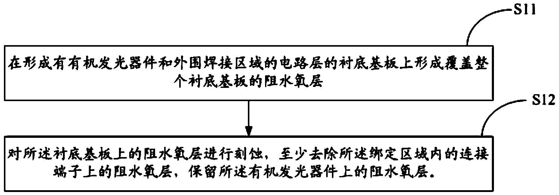
[0042] Method 1: remove all water and oxygen blocking layers in the binding area;
[0043] Method 2: remove the water-blocking oxygen layer on the connection terminals in the binding area, that is, retain the water-blocking oxygen layer outside the connection terminals.
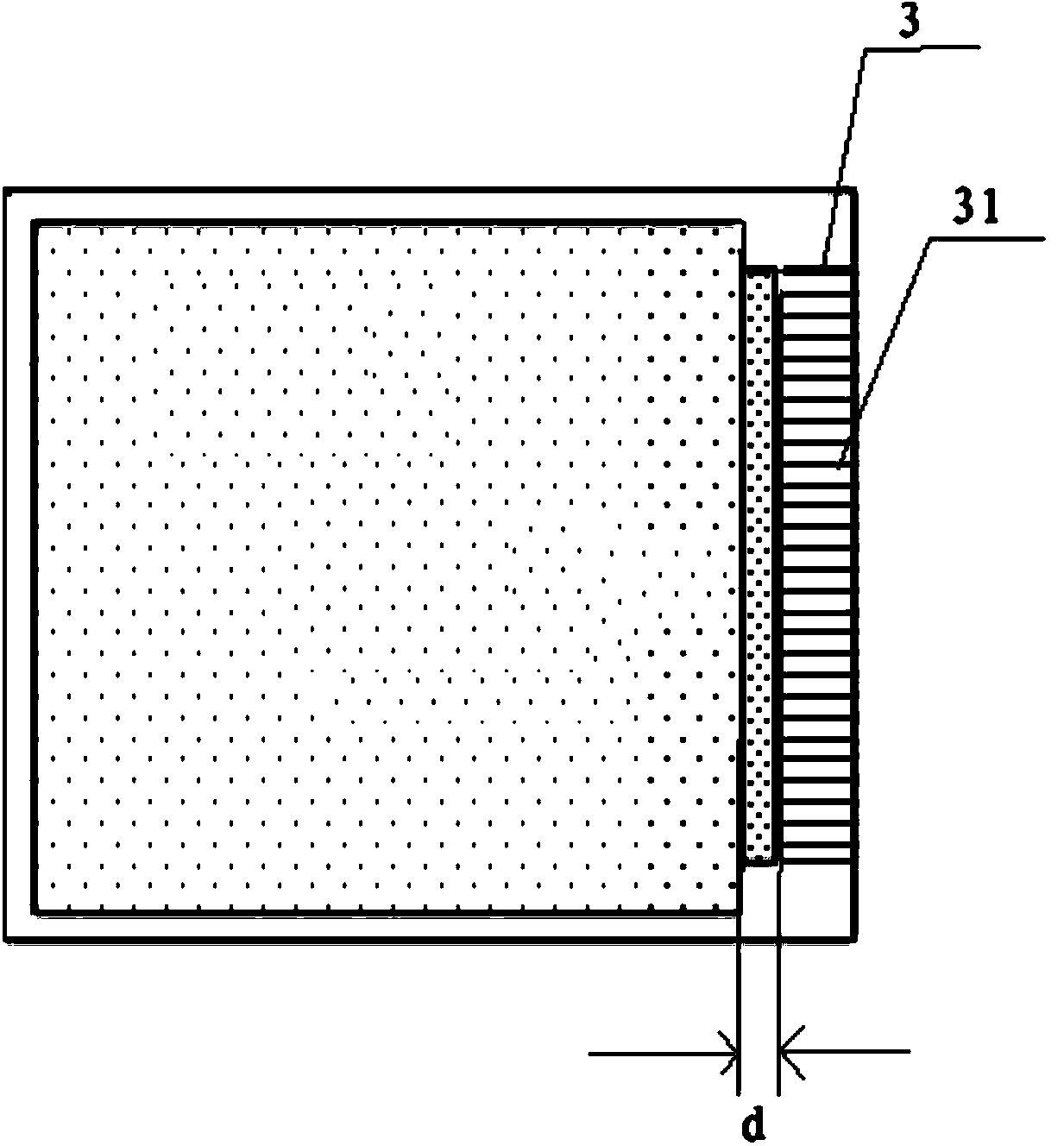
[0044] The size and setting position of the binding area of the organic light-emitting display panel are determined according to actual needs, for example, as figure 2 As shown, the size of the binding area 3 of the organic light emitting display panel may be equivalent to the area covered by the connection terminal 31 . The binding area 3 is located at an area extending a certain distance from the edge of the substrate to the center.
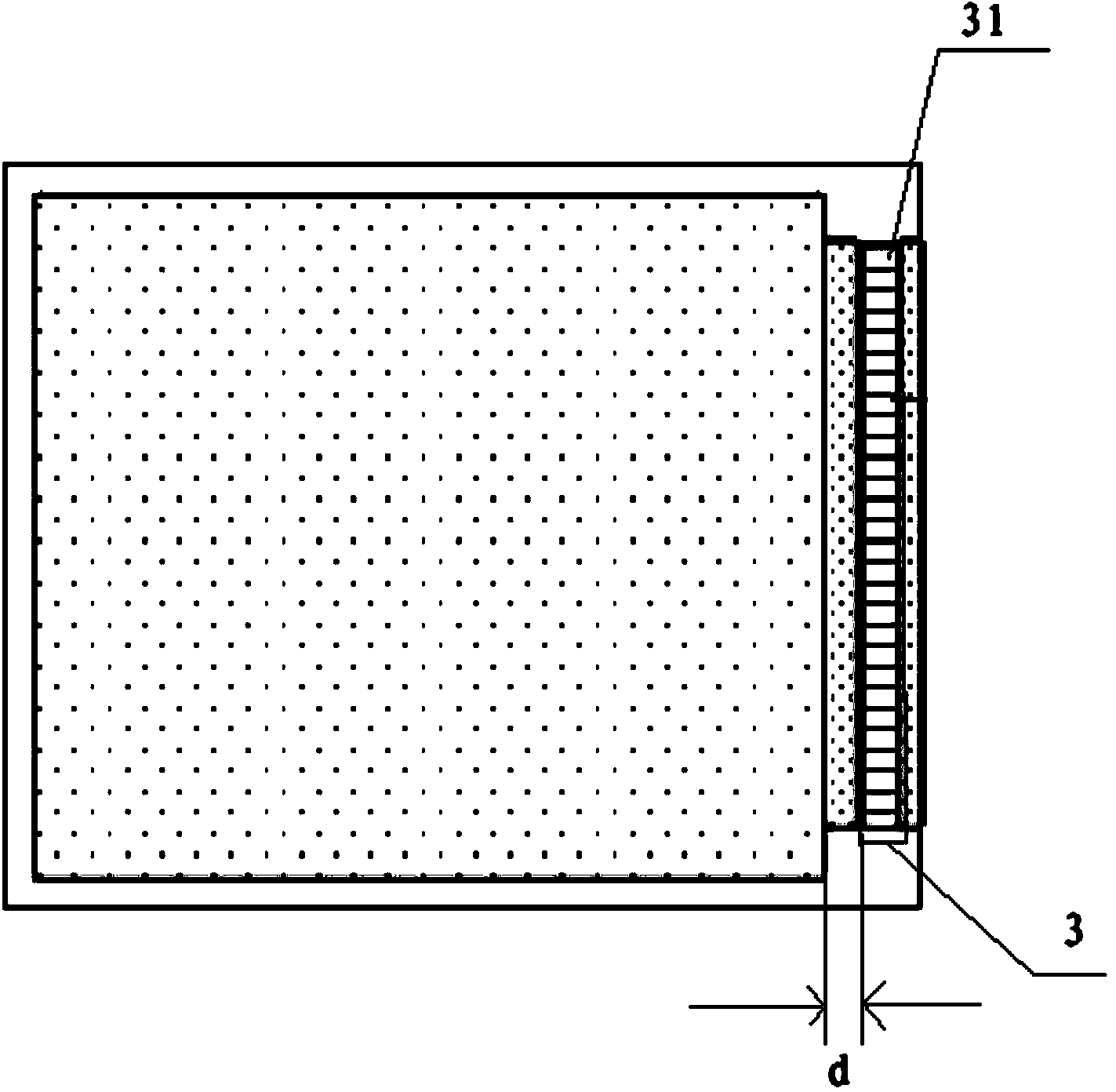
[0045] Such as image 3 As shown, the binding area 3 of the organic light emitting display panel is smaller than the area covered by the connecting terminal 31, and the binding area is a set distance away from the edge of the substrate.
[0046] In the specific implement...
PUM
 Abstract
Description
Claims
Application Information
 - R&D
- Intellectual Property
- Life Sciences
- Materials
- Tech Scout
- Unparalleled Data Quality
- Higher Quality Content
- 60% Fewer Hallucinations
Browse by: Latest US Patents, China's latest patents, Technical Efficacy Thesaurus, Application Domain, Technology Topic, Popular Technical Reports.
© 2025 PatSnap. All rights reserved.Legal|Privacy policy|Modern Slavery Act Transparency Statement|Sitemap|About US| Contact US: help@patsnap.com


