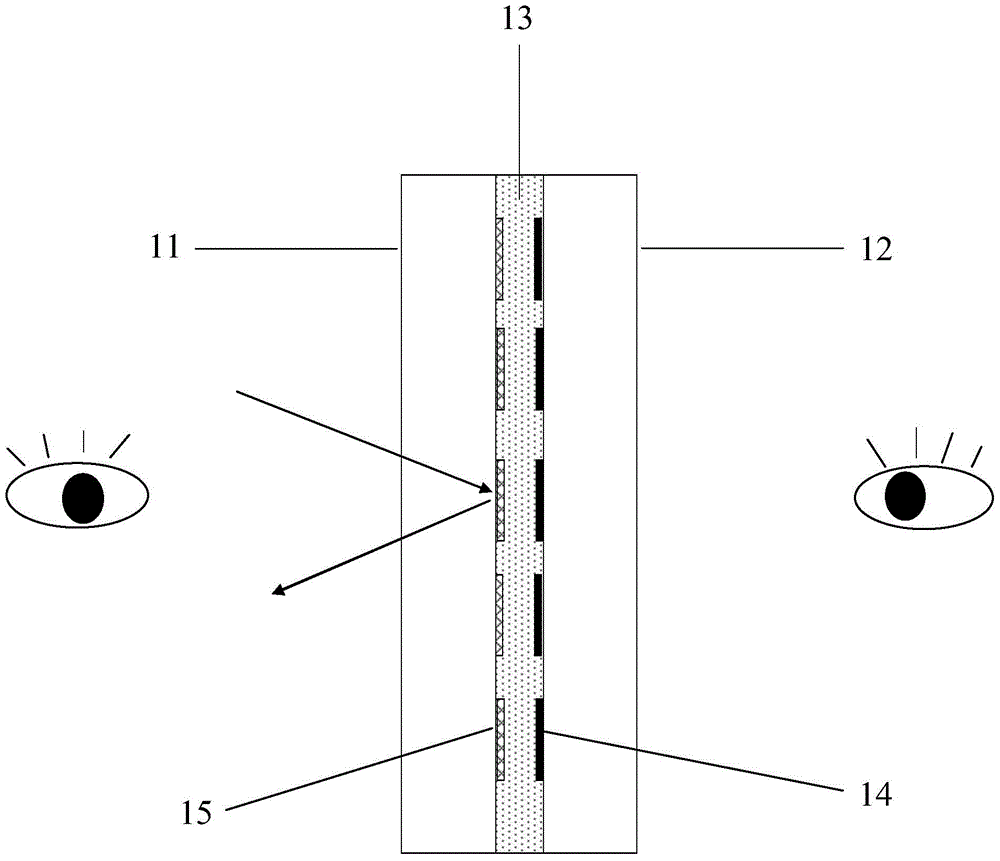
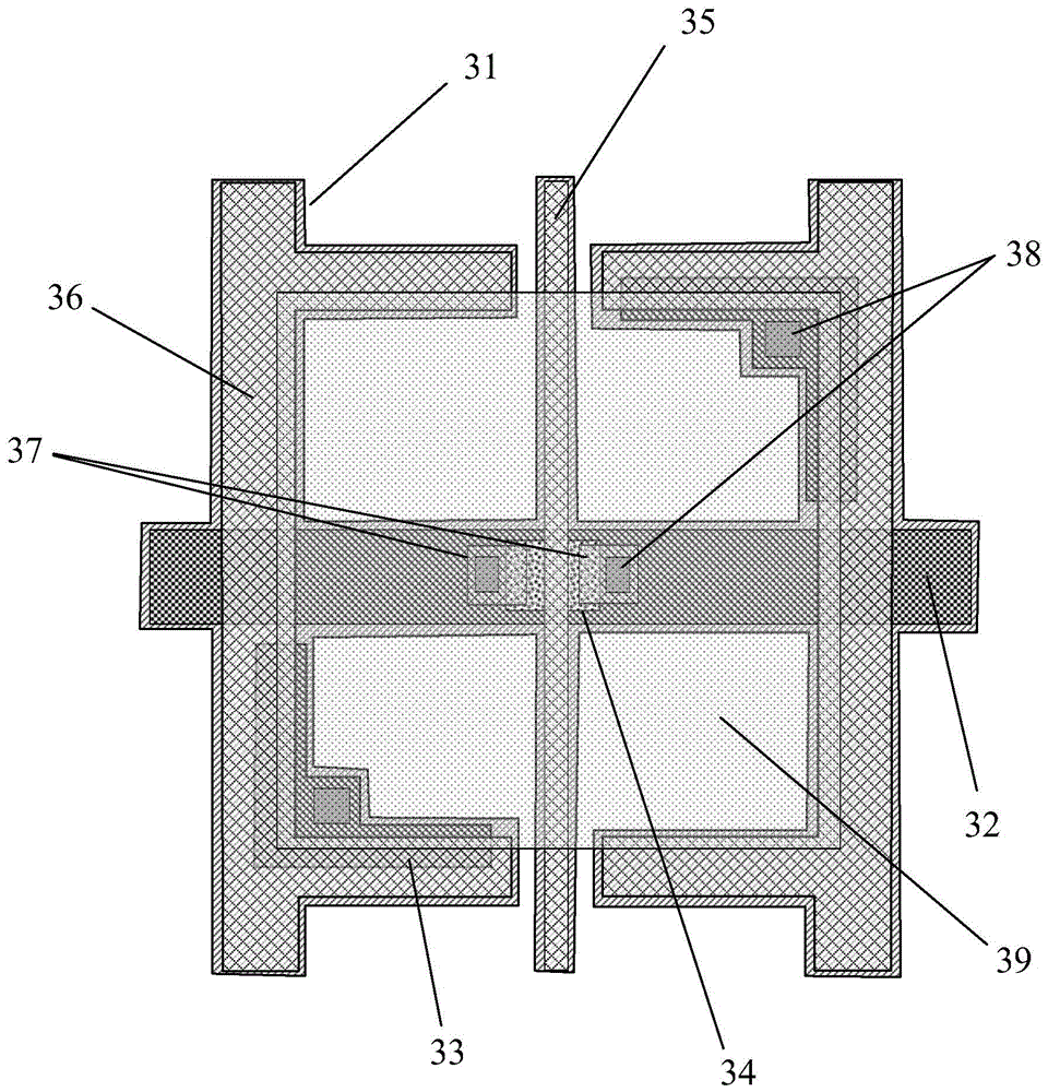
A double-sided transparent display device
A transparent display and double-sided technology, applied in nonlinear optics, instruments, optics, etc., can solve the problems of severe glare and low contrast, and achieve the same display effect
- Summary
- Abstract
- Description
- Claims
- Application Information
AI Technical Summary
Problems solved by technology
Method used
Image
Examples
Embodiment 1
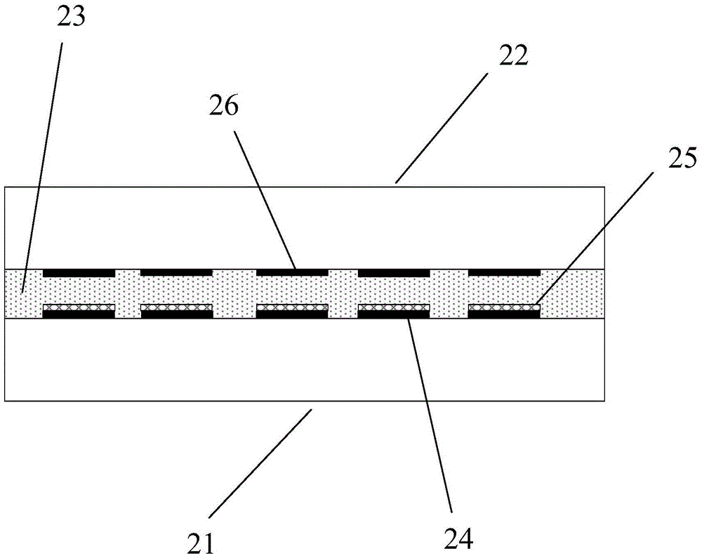
[0073] figure 2 It is a schematic structural diagram of a double-sided transparent display device according to the first embodiment of the present invention. like figure 2 As shown, a double-sided transparent display device includes: an array substrate 21, on which a first black matrix pattern 24 and a TFT array device 25 are sequentially arranged; A second black matrix pattern 26 is arranged on the side, and the second black matrix pattern 26 covers the TFT array device 25 ; a display medium layer 23 , such as liquid crystal, is sandwiched between the array substrate 21 and the opposite substrate 22 .
[0074] Wherein the TFT array device 25 is specifically provided on the array substrate in sequence with a first metal layer pattern, a first metal insulating layer, a semiconductor layer, a second metal layer pattern, a protective insulating layer, a transparent organic insulating film, and a pixel electrode. The first black matrix pattern covers the first and second metal...
Embodiment 2
[0089] Figure 10 It is a schematic structural diagram of a double-sided transparent display device according to the second embodiment of the present invention, Figure 10 As shown, the present invention provides a double-sided transparent display device, which includes: an array substrate 101, on which a first black matrix pattern 104, a TFT array device 105, and a second black matrix pattern 106 are sequentially arranged; 102, such as a color filter substrate; wherein, the patterns of the first and second black matrices 104 and 106 overlap and cover the TFT array device 105; a display medium layer 103, such as liquid crystal, is interposed between the array substrate 101 and the between the opposing substrates 102 .
[0090] see Figure 10 , 11 , wherein, the TFT array device 105 is specifically a first metal layer pattern, a first metal insulating layer, a semiconductor layer 114, a second metal layer pattern, a protective insulating layer, a transparent organic insulati...
Embodiment 3
[0108] Figure 15 It is the structure of the double-sided transparent display device according to the third embodiment of the present invention. like Figure 15 As shown, the present invention provides a double-sided transparent display device, which includes: an array substrate 151, which has two surfaces, and a first black matrix pattern 154 is arranged on one surface; Two black matrix patterns 156, a first metal layer pattern 154, a TFT array device 155; a pair of opposing substrates 152, such as a color filter substrate; wherein, the first and second black matrix patterns 154, 156 overlap and cover the TFT Array device 155 ; a display medium layer 153 , such as liquid crystal, interposed between the array substrate 151 and the opposite substrate 152 .
[0109] Wherein, the TFT array device 155 is specifically a first metal insulating layer, a semiconductor layer, a second metal layer pattern, a protective insulating layer, a transparent organic insulating film, and a pix...
PUM
| Property | Measurement | Unit |
|---|---|---|
| thickness | aaaaa | aaaaa |
Abstract
Description
Claims
Application Information
 - R&D Engineer
- R&D Manager
- IP Professional
- Industry Leading Data Capabilities
- Powerful AI technology
- Patent DNA Extraction
Browse by: Latest US Patents, China's latest patents, Technical Efficacy Thesaurus, Application Domain, Technology Topic, Popular Technical Reports.
© 2024 PatSnap. All rights reserved.Legal|Privacy policy|Modern Slavery Act Transparency Statement|Sitemap|About US| Contact US: help@patsnap.com


