A pm-oled cathode lead layout structure and manufacturing method thereof
A PM-OLED and cathode lead technology, applied in the field of PM-OLED, can solve the problems of high voltage drop and large resistance, and achieve the effect of reducing voltage drop, increasing width, and realizing narrow frame design
- Summary
- Abstract
- Description
- Claims
- Application Information
AI Technical Summary
Problems solved by technology
Method used
Image
Examples
Embodiment Construction
[0017] The present invention will be further described below in conjunction with accompanying drawing and specific embodiment:
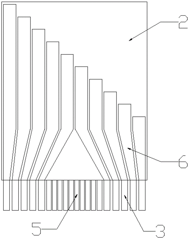
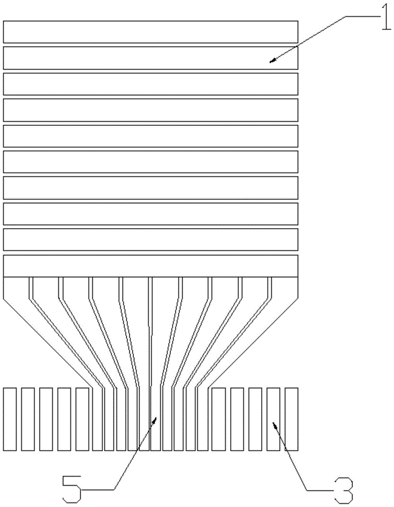
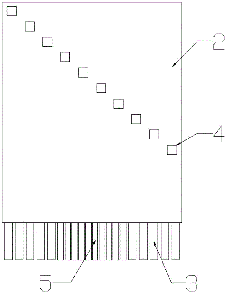
[0018] Such as figure 1 , figure 2 and image 3 As shown, the PM-OLED cathode lead layout structure of the present invention includes a cathode 1, a reserved cathode lead 3 and a cathode lead 6, the reserved cathode lead 3 is perpendicular to the cathode 1, the cathode 1 is covered with an insulating layer 2, and the insulating layer 2 Part of the anode lead 5 is also covered, and a cathode hole 4 is opened corresponding to each cathode lead 6 on the insulating layer 2, and the cathode holes 4 are distributed in steps, corresponding to each row of cathodes 1 one by one; the insulating layer 2 is a low-K material , and increase the thickness of the insulating layer 2 as much as possible within the range allowed by the process, the thicker low-K material insulating layer 2 can reduce the capacitive effect; one end of the cathode lead 6 is connected ...
PUM
 Abstract
Description
Claims
Application Information
 - Generate Ideas
- Intellectual Property
- Life Sciences
- Materials
- Tech Scout
- Unparalleled Data Quality
- Higher Quality Content
- 60% Fewer Hallucinations
Browse by: Latest US Patents, China's latest patents, Technical Efficacy Thesaurus, Application Domain, Technology Topic, Popular Technical Reports.
© 2025 PatSnap. All rights reserved.Legal|Privacy policy|Modern Slavery Act Transparency Statement|Sitemap|About US| Contact US: help@patsnap.com


