Display substrate and manufacturing method thereof, display panel and display device

A technology for displaying substrates and manufacturing methods, applied in instruments, nonlinear optics, optics, etc., can solve problems such as narrow borders, reduce possibilities, increase production costs, and achieve the effect of narrow border design

Active Publication Date: 2017-01-18
BOE TECH GRP CO LTD +1
View PDF11 Cites 0 Cited by
  • Summary
  • Abstract
  • Description
  • Claims
  • Application Information

AI Technical Summary

Problems solved by technology

[0005] The technical problems to be solved by the present invention include, aiming at the problem that the frame of the existing display panel is relatively wide, providing a display substrate, a manufacturing method thereof, and a display panel, and a display device including the above-mentioned display panel has a relatively narrow frame

Method used


Image

  • Display substrate and manufacturing method thereof, display panel and display device
  • Display substrate and manufacturing method thereof, display panel and display device
  • Display substrate and manufacturing method thereof, display panel and display device

Examples


Embodiment 1

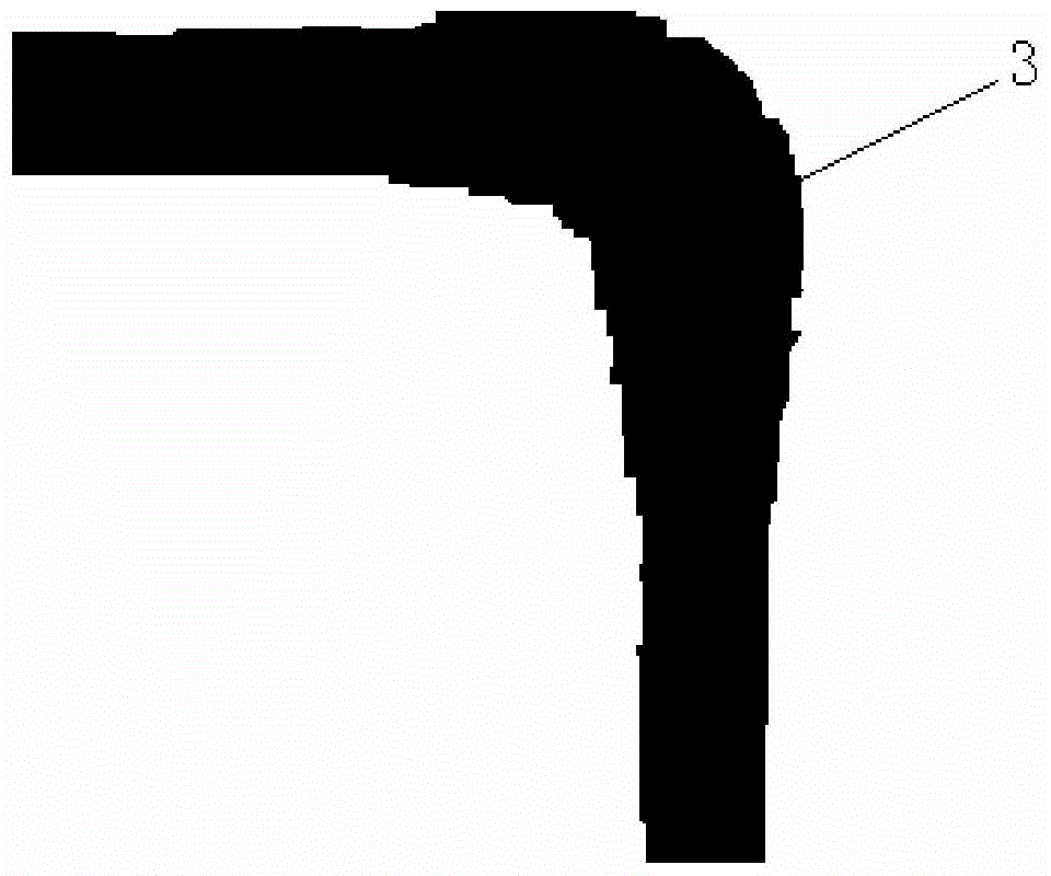
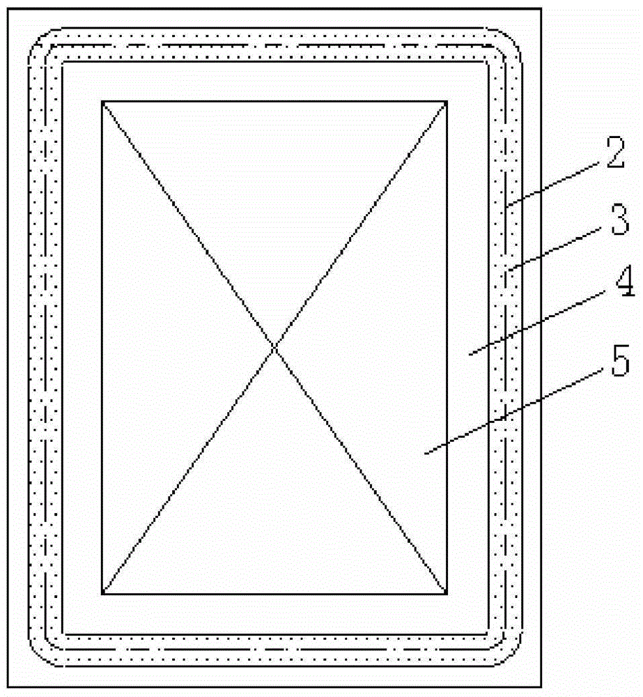
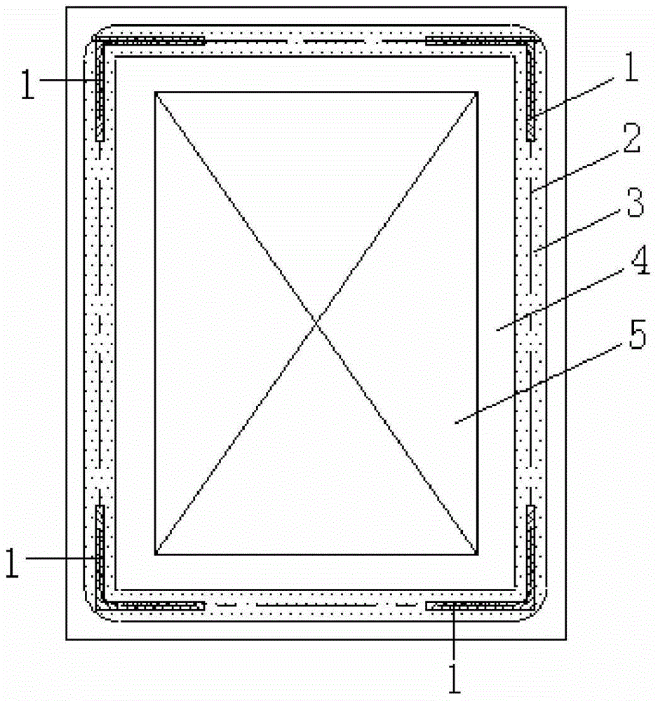
[0036] This embodiment provides a display substrate, which can be an array substrate or a color filter substrate, and can be used to make a display panel, such as a liquid crystal display panel. , it is necessary to coat the sealant on the display substrate, all of which can be applied to the display substrate of the embodiment of the present invention. Such as Figures 3 to 5 As shown, the display substrate of this embodiment includes a substrate, which can be a glass or quartz substrate, and the substrate includes a display area 5 and a non-display area 4 (for arranging lead joints, etc.) located around the display area 5, wherein the display area 5 There are various pixel structures for displaying in the center, and the non-display area 4 is arranged around the display area 5 for arranging lead joints, coating sealant, and the like. In the non-display area 4, there is a frame sealant coating area 2, which is used to coat the frame sealant to realize the box alignment of th...

Embodiment 2

[0070] This embodiment provides a display panel, which includes a first substrate, and the display panel further includes the display substrate in Embodiment 1.

[0071] Preferably, the first substrate is an array substrate, and the display substrate is a color filter substrate; or the first substrate is a color filter substrate, and the display substrate is an array substrate.

[0072] This embodiment also provides a manufacturing method for the above-mentioned display panel (taking the display panel as an example of a liquid crystal display panel), including the following steps:

[0073] Such as Figures 3 to 5 As shown, the frame sealant 3 is coated on the frame sealant coating area 2 of the display substrate (that is, the color filter substrate) in Example 1, wherein the frame sealant 3 is formed above at least part of the raised structure 1;

[0074] Drop liquid crystal into the display area of ​​the first substrate (at this time, the array substrate);

[0075] Carrying...


PUM


Abstract

The invention provides a display substrate, a manufacturing method thereof, a display panel and a display device, belongs to the field of display techniques and can solve the problem that the frame of the existing display panel is wide. The display substrate provided by the invention comprises a base, wherein a frame sealing adhesive coating area is arranged on the base, the frame sealing adhesive coating area is provided with a plurality of corner parts and convex structures are arranged at the corner parts of the frame sealing adhesive coating area. The manufacturing method of the display substrate comprises the step of forming the convex structures at the corner parts of the frame sealing adhesive coating area of the base through a pattern forming technology. The display panel provided by the invention comprises the display substrate. The display substrate can be used for manufacturing the display device.

Description

technical field [0001] The invention belongs to the field of display technology, and in particular relates to a display substrate and a manufacturing method thereof, a display panel and a display device. Background technique [0002] Thin Film Transistor Liquid Crystal Display (TFT-LCD) has the advantages of small size, low power consumption, no radiation, and high resolution. It occupies a dominant position in the current display field and has been widely used in modern In digital information equipment. With the rapid development of flat panel display technology, narrow bezel liquid crystal display products are increasingly favored by consumers. [0003] TFT liquid crystal displays generally include two parts: a backlight module and a liquid crystal display panel. The liquid crystal display panel includes a first substrate and a second substrate and a liquid crystal layer arranged between the first substrate and the second substrate; one of the first substrate and the sec...

Claims


Application Information

Patent Timeline
Patent Type & Authority Patents(China)
IPC IPC(8): G02F1/1333G02F1/1339
Inventor 姜妮
Owner BOE TECH GRP CO LTD
Why Eureka
Try Eureka