Testing structure and testing method

A technology for testing structures and conductive structures, which is applied in semiconductor/solid-state device testing/measurement, electrical components, electric solid-state devices, etc., and can solve problems such as increased test difficulty and extended test time

Active Publication Date: 2014-05-21
SHANGHAI HUAHONG GRACE SEMICON MFG CORP
View PDF3 Cites 4 Cited by
  • Summary
  • Abstract
  • Description
  • Claims
  • Application Information

AI Technical Summary

Problems solved by technology

[0007] However, using the existing test structure to test the probe resistance will increase the difficulty of the test, which will lead to a longer test time

Method used


Image

  • Testing structure and testing method
  • Testing structure and testing method
  • Testing structure and testing method

Examples


Embodiment Construction

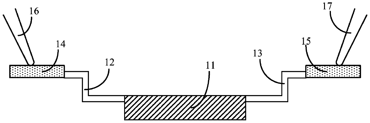
[0036] As mentioned in the background art, using the existing test structure to test the resistance of the probe will increase the difficulty of the test, thereby prolonging the test time.

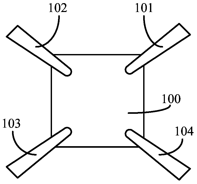
[0037] After research, please refer to figure 2 , figure 2It is a schematic top view of a test structure for testing probe resistance, including a test pad 100, the material of which is a conductive material, and the test pad 100 is a square. When testing, the first probe 101, the second probe 102, the third probe 103 and the fourth probe 104 are placed on the surface of the test pad 100 together to realize the first probe 101, the second probe Electrical interconnection between needle 102 , third probe 103 and fourth probe 104 . By applying different bias voltages to the first probe 101, the second probe 102, the third probe 103, and the fourth probe 104, the corresponding currents are obtained, and the first probes are respectively obtained through the relationship between voltage an...


PUM


Abstract

The invention discloses a testing structure and a testing method. The testing structure comprises a symmetrical conducting structure, the symmetrical conducting structure is parallel to a pattern along the surface of a substrate and has a first axis and a second axis, the first axis and the second axis are vertical to each other, portions of the symmetrical conducting structure positioned on both sides of the first axis are symmetrical to each other, portions of the symmetrical conducting structure positioned on both sides of the second axis are symmetrical to each other, and a portion of the symmetrical conducting structure positioned on one side of the first axis is the same as a portion of the symmetrical conducting structure positioned on one side of the second axis. The testing structure further comprises a first lead, a second lead, a third lead and a fourth lead, wherein the first ends of the first lead and the fourth lead are connected with the two ends of the symmetrical conducting structure along the first axis respectively; the first ends of the second lead and the third lead are connected with the two ends of the symmetrical conducting structure along the second axis respectively; the first lead, the second lead, the third lead and the fourth layer are the same in resistance. By adopting the testing structure, the probe resistance testing difficulty can be lowered, and the testing time is shortened.

Description

technical field [0001] The invention relates to the technical field of semiconductor manufacturing, in particular to a test structure and a test method. Background technique [0002] In the semiconductor manufacturing process, it is often necessary to conduct parameter tests or reliability tests on semiconductor devices through probes, such as current-voltage (I-V) tests and constant temperature electro-migration tests (Isothermal Electro-migration Test), to characterize the performance of semiconductor devices and reliability. [0003] Take the test of the resistance of semiconductor devices with probes as an example, please refer to figure 1 , figure 1 It is a schematic cross-sectional structure diagram of testing the resistance of a semiconductor device through a probe, including: a device 11 formed on the surface of a semiconductor substrate (not shown); a first wire 12 and a second wire respectively located at both ends of the device 11 13, the first wire 12 and the ...

Claims


Application Information

Patent Timeline
IPC IPC(8): H01L23/544H01L21/66
Inventor 范象泉
Owner SHANGHAI HUAHONG GRACE SEMICON MFG CORP
Why Eureka
Try Eureka