Method for measuring bias and gain errors of time alternative ADC acquisition system
A technology of acquisition system and gain error, applied in the direction of analog/digital conversion calibration/test, etc., can solve the problems of channel mismatch, gain, offset and time offset error, etc.
- Summary
- Abstract
- Description
- Claims
- Application Information
AI Technical Summary
Problems solved by technology
Method used
Image
Examples
Embodiment
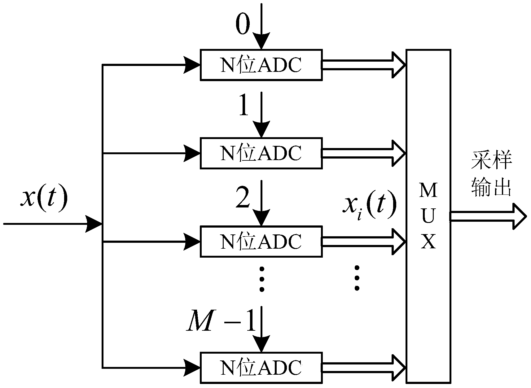
[0034] figure 1 It is a functional block diagram of the method for measuring the offset and gain errors of a time-alternating ADC acquisition system in the present invention.
[0035] In this example, if figure 1 As shown, let the input signal be x(t)=Acos(2πf in t+φ in ), where the magnitude of x(t) is A and the frequency is f in , the initial phase is φ in , the present invention measures the method for time-alternating ADC acquisition system offset and gain error, comprises the following steps:
[0036] (1), the signal is x(t)=Acos(2πf in t+φ in ) is input to the time-alternating ADC acquisition system, where, L is the number of FFT points, and L is the positive integer power of 2, that is, L=2 m , m is a positive integer, f s is the equivalent sampling rate of the system, P is a positive integer, and is relatively prime to L, that is, only one common divisor of L and P is 1, and the output signal x is processed by the TIADC acquisition system i (t), i=0,1,...,M-...
PUM
 Abstract
Description
Claims
Application Information
 - R&D
- Intellectual Property
- Life Sciences
- Materials
- Tech Scout
- Unparalleled Data Quality
- Higher Quality Content
- 60% Fewer Hallucinations
Browse by: Latest US Patents, China's latest patents, Technical Efficacy Thesaurus, Application Domain, Technology Topic, Popular Technical Reports.
© 2025 PatSnap. All rights reserved.Legal|Privacy policy|Modern Slavery Act Transparency Statement|Sitemap|About US| Contact US: help@patsnap.com


