Voltage boost circuit, shift register and gate driving module
A shift register and voltage boosting technology, applied in static memory, digital memory information, instruments, etc., can solve the problem that the driving circuit cannot be applied to the stereoscopic image display device.
- Summary
- Abstract
- Description
- Claims
- Application Information
AI Technical Summary
Problems solved by technology
Method used
Image

Examples
Embodiment Construction
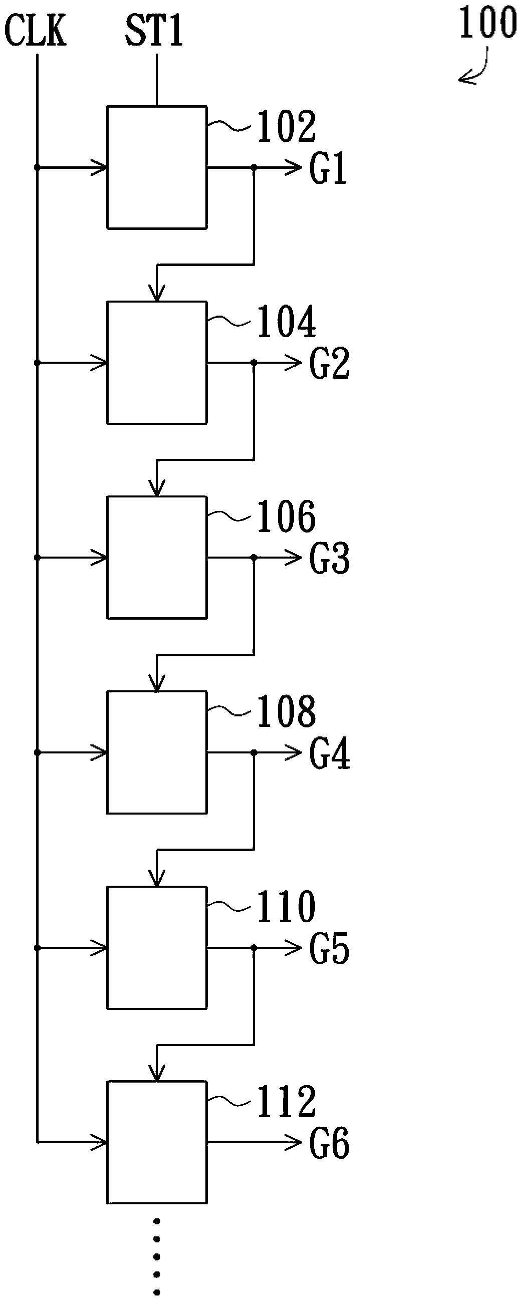
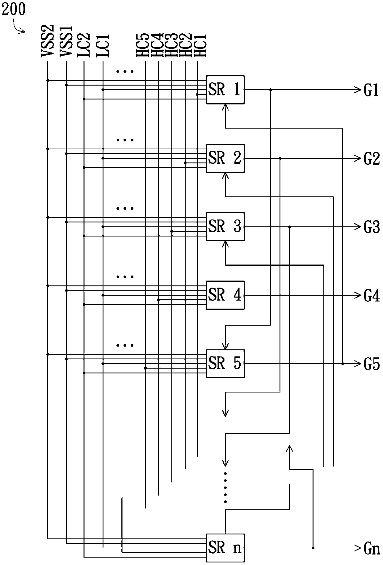
[0045] figure 2 A circuit block diagram of a gate driving module used in a display device according to a preferred embodiment of the present invention is shown. Please refer to figure 2 , the gate driving module 200 provided in this embodiment includes a plurality of shift registers SR1 , SR2 , SR3 , SR4 , SR5 . . . , SRn arranged in sequence. Wherein, each shift register outputs a gate signal G1 , G2 , G3 , G4 , G5 . . . , Gn to scan the corresponding gate line in the display device. In addition, in this embodiment, each shift register is coupled to a clock signal, for example image 3 Shown are HC1, HC2, HC3, HC4, HC5....
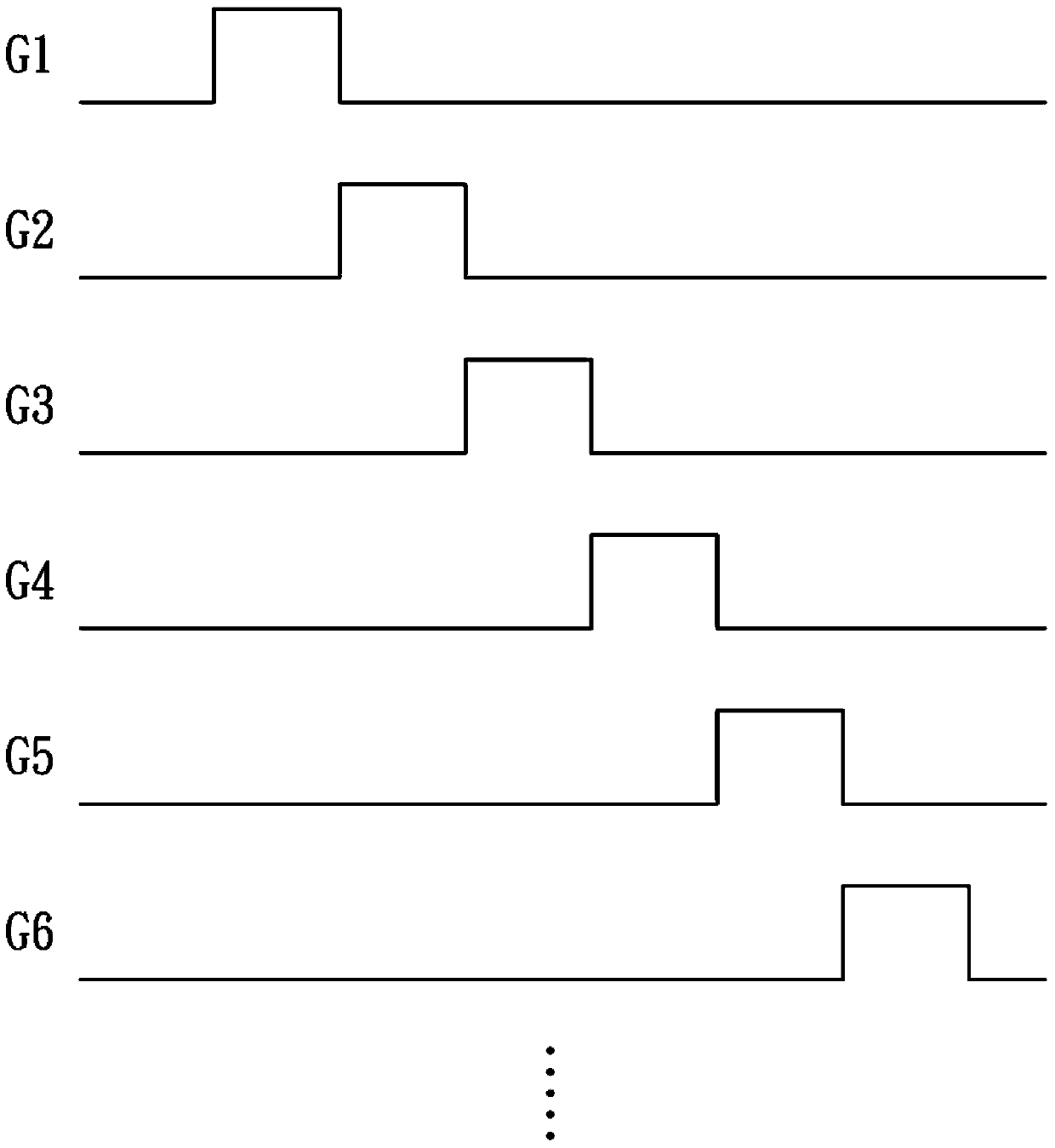
[0046] image 3 A timing diagram of a clock signal of a display device in a stereoscopic image display mode is shown according to an embodiment of the present invention. Please merge reference figure 2 and image 3 , when the display device is displaying stereoscopic images (that is, working in 3D mode), since the left-eye signal and the right-e...
PUM
 Abstract
Description
Claims
Application Information
 - Generate Ideas
- Intellectual Property
- Life Sciences
- Materials
- Tech Scout
- Unparalleled Data Quality
- Higher Quality Content
- 60% Fewer Hallucinations
Browse by: Latest US Patents, China's latest patents, Technical Efficacy Thesaurus, Application Domain, Technology Topic, Popular Technical Reports.
© 2025 PatSnap. All rights reserved.Legal|Privacy policy|Modern Slavery Act Transparency Statement|Sitemap|About US| Contact US: help@patsnap.com