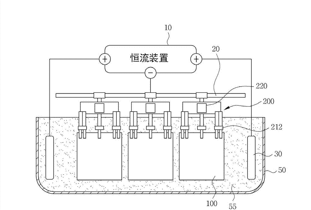
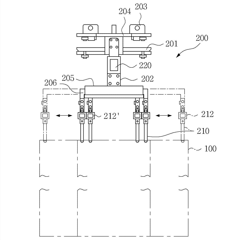
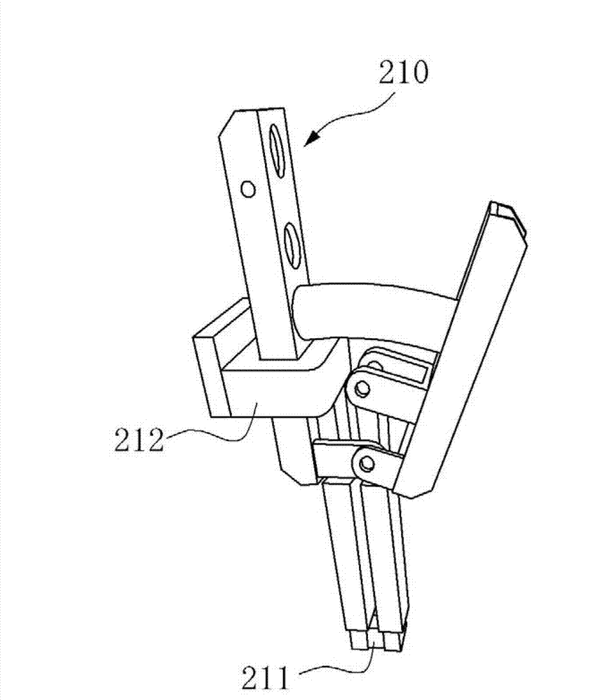
Substrate plating apparatus and substrate plating control method
A technology of electroplating equipment and control methods, which is applied in the fields of printed circuit manufacturing, electrical components, electrolytic process, etc., and can solve the problems of reduced surface quality, uneven plating thickness, uneven distribution of plating thickness, etc.
- Summary
- Abstract
- Description
- Claims
- Application Information
AI Technical Summary
Problems solved by technology
Method used
Image

Examples
Embodiment Construction
[0037] The objects, features and advantages of the present invention will be more clearly understood from the following description of the embodiments with reference to the accompanying drawings.
[0038] The terms and words used in the description and claims of the present invention should not be construed as being limited to the usual meanings or dictionary definitions, but should be understood as based on the rules on which the inventors can properly define the concepts of terms, these terms and Words have meanings and concepts related to the technical scope of the present invention to best describe his or her known methods for carrying out the present invention.
[0039] The above and other objects, features and advantages of the present invention can be more clearly understood through the following detailed description in conjunction with the accompanying drawings. In the specification, in adding reference numerals to different components in the drawings, it should be not...
PUM
 Abstract
Description
Claims
Application Information
 - R&D
- Intellectual Property
- Life Sciences
- Materials
- Tech Scout
- Unparalleled Data Quality
- Higher Quality Content
- 60% Fewer Hallucinations
Browse by: Latest US Patents, China's latest patents, Technical Efficacy Thesaurus, Application Domain, Technology Topic, Popular Technical Reports.
© 2025 PatSnap. All rights reserved.Legal|Privacy policy|Modern Slavery Act Transparency Statement|Sitemap|About US| Contact US: help@patsnap.com