
Methodology of forming optical lens for semiconductor light emitting device

A technology of optical lens and light-emitting device, which is applied in the direction of semiconductor devices, electric solid-state devices, electrical components, etc., and can solve the problems of light output loss, yield loss, packaging material waste, etc.

Inactive Publication Date: 2013-05-22
INTERQUARTZ TAIWAN
View PDF3 Cites 3 Cited by
  • Summary
  • Abstract
  • Description
  • Claims
  • Application Information

AI Technical Summary

Problems solved by technology

Furthermore, yield loss issues can result due to encapsulation material delaminating in planar areas or chips and detaching from support structures
Other disadvantages are loss of light output due to coupling light out of unwanted areas through the planar area, and unnecessary waste of expensive encapsulation material in the planar area

Method used


Image

  • Methodology of forming optical lens for semiconductor light emitting device
  • Methodology of forming optical lens for semiconductor light emitting device
  • Methodology of forming optical lens for semiconductor light emitting device

Examples


Embodiment Construction

[0039] In the detailed description that follows, numerous specific details are set forth in order to provide a thorough understanding of the invention. However, it will be understood by those skilled in the art that the present invention may be practiced without these specific details. In other instances, well-known methods, procedures and / or components have not been described in detail so as not to obscure the present invention.

[0040] The present invention will be more clearly understood by the following description of the examples, given by way of example only by reference to the accompanying drawings, which are not drawn to scale.

[0041] refer to Figure 1-A , a schematic diagram showing a conventional method of forming an optical lens for a semiconductor light emitting device by using an injection molding process. A quantity of encapsulant material is spread over a mold provided with depressions or cavities corresponding to the desired lens shape. By applying pressu...


PUM

PropertyMeasurementUnit
Surface energyaaaaaaaaaa

Abstract

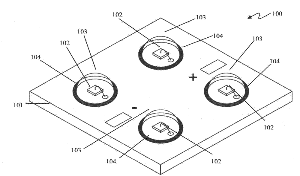
The present invention relates generally to a methodology of forming optical lens (103) on support structure (101) for semiconductor light emitting device (100) by applying low surface energy barrier band or surface (104) onto said support structure (101). Said optical lens (103) is used as an encapsulation over semiconductor light emitting die (102) to shape and extract light out from the semiconductor light emitting die (102), as well as to provide protection from mechanical damage and environmental influence.

Description

1. Technical field [0001] The present invention generally relates to methods of forming optical lenses for semiconductor light emitting devices on a support structure by applying a low surface energy barrier strip or surface to the support structure. 2. Background technology [0002] Semiconductor light emitting devices such as light emitting diodes (LEDs) are semiconductor light sources that have been used in several fields of application over the past few decades. Improvements to LEDs continue in the areas of efficiency, brightness and manufacturing processes. In surface mount LEDs, the LED die is mounted on a support structure and encapsulated in an optical dome lens to protect it from mechanical damage, environmental influences, and to form and extract light away from the LED die. [0003] There are several methods used in the industry to form optical lenses. Common types of lenses for surface mount LEDs can be formed using injection molding or extrusion molding proces...

Claims


Application Information

Patent Timeline
IPC IPC(8): H01L33/58H01L33/52H01L33/48
CPCH01L33/54H01L33/44H01L2933/005H01L2224/48091H01L2924/00014
Inventor 郭学钦
Owner INTERQUARTZ TAIWAN
Learn More