
Power and area efficient interleaved ADC

A multiplexer, hold circuit technology, applied in the direction of analog/digital conversion, code conversion, electrical components, etc., can solve problems such as doubling power consumption and increasing noise

Active Publication Date: 2013-04-17
TEXAS INSTR INC
View PDF12 Cites 4 Cited by
  • Summary
  • Abstract
  • Description
  • Claims
  • Application Information

AI Technical Summary

Problems solved by technology

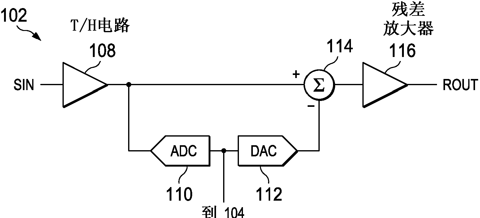
This arrangement allows relaxed timing because the sampled signal is held for the entire period of the clock signal CLK, but the addition of the T / H circuit 206 adds noise (ie, 3dB per T / H circuit 206)
To compensate for noise degradation, the power consumption of each T / H circuit 108 and 206 is doubled, resulting in four times the power consumption of a single T / H system

Method used


Image

  • Power and area efficient interleaved ADC
  • Power and area efficient interleaved ADC
  • Power and area efficient interleaved ADC

Examples


Embodiment Construction

[0027] exist Figure 3A In , an ADC 300 according to an exemplary embodiment of the present invention is presented. ADC 300 has substantially the same functionality as ADC 100 . However, there is a difference in the pipeline; that is, stages 102-1 to 102-N are replaced by stages 302-1 to 302-N and clock circuit 303.

[0028] refer to Figure 3B and Figure 3C, stages 302-1 to 302-N (hereinafter 302) can be seen in more detail. In operation, T / H circuits 304 and 306 are coupled to receive an analog input signal (analog input signal AIN or a residual signal from a previous stage). Since these T / H circuits 304 and 306 are arranged in parallel with each other, the timing of the T / H circuits 304 and 306 can be designed such that sampling occurs on substantially non-overlapping logic stages or phases of the clock signal. Preferably, the clock circuit 303 generally includes a clock divider (ie, a clock divider with a frequency divided by 2) to generate a clock signal CLK / 2 with a...


PUM


Abstract

Pipeline analog-to-digital converters (ADCs) are commonly used for high frequency applications; however, operating at high sampling rates will often result in high power consumption or tight timing constraints. Here, though, an ADC is provided that allows for relaxed timing (which enables a high sampling rate) with low power consumption. This is accomplished through the use of multiplexed, front-end track- and-hold (T / H) circuits that sample on non-overlapping portions of a clocking signal in conjunction with ''re-used'' or shared analog processing circuitry. Parallel track- and-hold (T / H) circuits (304, 306) receive an analog input signal (AIN or prior residue) and are clocked at half clock cycles (CLK / 2) by clocking circuit 303 to sample / hold on non- overlapping logic phases. The T / H circuits (304, 306) are respectively coupled to analog-to-digital converter (ADC 310) through multiplexer (308) and to digital-to-analog converter (DAC 312), adder (314) and amplifier (316) to perform analog processing to resolve sampled signals for digital output circuit (104) and to generate a residue signal (ROUT).

Description

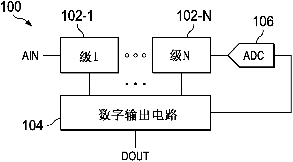
technical field [0001] The present invention relates generally to analog-to-digital converters (ADCs), and more particularly to interleaved ADCs. Background technique [0002] High-performance ADCs typically do not obey the "Moore's Law" area and power curves of digital circuit implementations in ever-shrinking CMOS process technologies. The ADC's noise and resolution requirements dictate power constraints (lower noise requires higher power) and area constraints (exceeding parts matching requirements). Also, as ADC sampling rates increase, typical architectures cannot provide the required performance due to timing constraints. [0003] Referring to FIG. 1A of the drawings, reference numeral 100 generally designates a conventional ADC 100 . ADC 100 typically includes several stages 102 - 1 through 102 -N, ADC 106 (which is typically a flash ADC), and digital output circuitry 104 . Stages 102-1 through 102-N are typically coupled in series with one another in a sequence whe...

Claims


Application Information

Patent Timeline
IPC IPC(8): H03M1/12
CPCH03M1/1215H03M1/1225H03M1/164H03M1/44
Inventor W·J·布赖特R·F·佩恩
Owner TEXAS INSTR INC
Learn More