A strained Si vertical back-channel nano-CMOS integrated device and its preparation method
A vertical channel and integrated device technology, which is applied in semiconductor/solid-state device manufacturing, nanotechnology, nanotechnology, etc., can solve the problems of increasing the difficulty of process manufacturing and limited adjustment range of device threshold voltage, so as to increase integration and improve Current drive capability, cost reduction effect
- Summary
- Abstract
- Description
- Claims
- Application Information
AI Technical Summary
Problems solved by technology
Method used
Image

Examples
Embodiment 1
[0053] Embodiment 1: the strained Si back-type channel CMOS integrated device and circuit that the preparation conduction channel is 45nm, concrete steps are as follows:
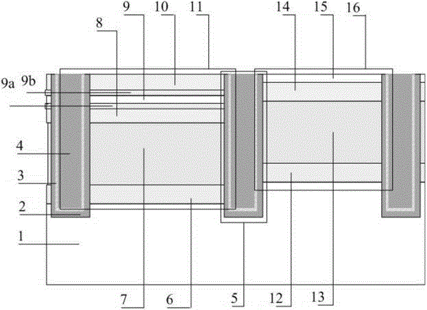
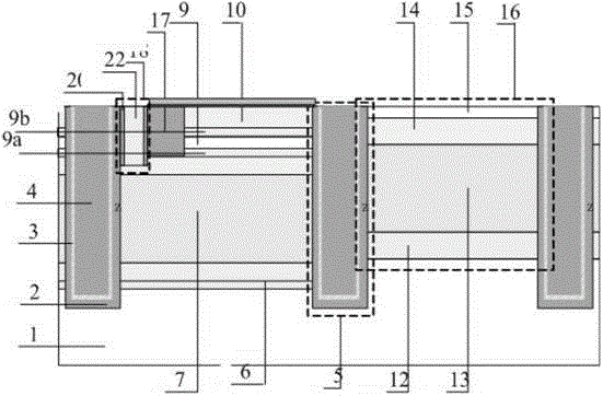
[0054] Step 1, isolation preparation of MOS active region, such as figure 2 , image 3 shown.
[0055] (1a) Select the doping concentration to be 5×10 15 cm -3 An N-type Si substrate sheet 1;
[0056] (1b) using a dry etching process to etch a deep groove with a depth of 3.5 μm in the isolation region;
[0057] (1c) Deposit the first SiO with a thickness of 20 nm on the surface of the substrate at 600 ° C by chemical vapor deposition (CVD) method 2 Layer 2, covering all the inner surface of the deep groove;
[0058] (1d) Deposit a SiN layer 3 with a thickness of 50 nm in the deep groove at 600° C. by chemical vapor deposition (CVD);
[0059] (1e) Deposit SiO in deep trenches at 600 °C by chemical vapor deposition (CVD) 2 4. Form deep trench isolation 5.
[0060] Step 2, PMOS active region epitaxial...
Embodiment 2
[0099] Embodiment 2: the preparation of the strained Si back-type structure CMOS integrated device and circuit with a conductive channel of 30nm, the specific steps are as follows:
[0100] Step 1, isolation preparation of MOS active region, such as figure 2 , image 3 shown.
[0101] (1a) Select the doping concentration as 3×10 15 cm -3 An N-type Si substrate sheet 1;
[0102] (1b) using a dry etching process to etch a deep groove with a depth of 3 μm in the isolation region;
[0103] (1c) Deposit the first SiO with a thickness of 30nm on the surface of the substrate at 700°C by chemical vapor deposition (CVD) 2 Layer 2, covering all the inner surface of the deep groove;
[0104] (1d) Deposit a SiN layer 3 with a thickness of 80 nm in the deep trench at 700° C. by chemical vapor deposition (CVD);
[0105] (1e) Deposit SiO in deep trenches at 700 °C by chemical vapor deposition (CVD) 2 4. Form deep trench isolation 5.
[0106] Step 2, PMOS active region epitaxial mat...
Embodiment 3
[0145] Embodiment 3: prepare the strained Si back-type structure CMOS integrated device and the circuit that the conductive channel is 22nm, the specific steps are as follows:
[0146] Step 1, isolation preparation of MOS active region, such as figure 2 , image 3 shown.
[0147] (1a) Select the doping concentration as 1×10 15 cm -3 An N-type Si substrate sheet 1;
[0148] (1b) using a dry etching process to etch a deep groove with a depth of 2.5 μm in the isolation region;
[0149] (1c) Deposit the first SiO with a thickness of 40 nm on the surface of the substrate at 800 ° C by chemical vapor deposition (CVD) method 2 Layer 2, covering all the inner surface of the deep groove;
[0150] (1d) Deposit a SiN layer 3 with a thickness of 100 nm in the deep trench at 800° C. by chemical vapor deposition (CVD);
[0151] (1e) Deposit SiO in deep trenches at 800 °C by chemical vapor deposition (CVD) 2 4. Form deep trench isolation 5.
[0152] Step 2, PMOS active region epita...
PUM
| Property | Measurement | Unit |
|---|---|---|
| thickness | aaaaa | aaaaa |
| thickness | aaaaa | aaaaa |
| thickness | aaaaa | aaaaa |
Abstract
Description
Claims
Application Information
 - R&D
- Intellectual Property
- Life Sciences
- Materials
- Tech Scout
- Unparalleled Data Quality
- Higher Quality Content
- 60% Fewer Hallucinations
Browse by: Latest US Patents, China's latest patents, Technical Efficacy Thesaurus, Application Domain, Technology Topic, Popular Technical Reports.
© 2025 PatSnap. All rights reserved.Legal|Privacy policy|Modern Slavery Act Transparency Statement|Sitemap|About US| Contact US: help@patsnap.com