Wiring structure of induction layer
A wiring structure and sensing layer technology, applied in the field of wiring structure of capacitive touch screen sensing layer, can solve problems such as poor capacitive coupling and decreased sensitivity of capacitive touch screen, and achieve the effect of solving the floating problem, flexible design and strong adaptability
- Summary
- Abstract
- Description
- Claims
- Application Information
AI Technical Summary
Problems solved by technology
Method used
Image
Examples
Embodiment Construction
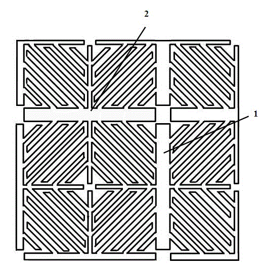
[0012] The present invention will be further described below in conjunction with the accompanying drawings and embodiments.
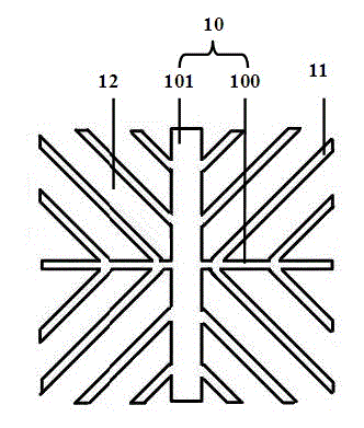
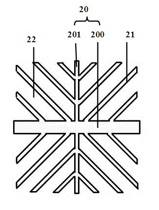
[0013] Such as Figure 1 to Figure 5 As shown, the present invention relates to a wiring structure of a sensing layer, the sensing layer includes a first sensing electrode 1 and a second sensing electrode 2, and the first sensing electrodes 1 and the second sensing electrodes 2 are arranged alternately, so The first sensing electrodes 1 are connected vertically, and the second sensing electrodes 2 are connected horizontally. The first sensing electrodes and the second sensing electrodes may be arranged in a single layer on both sides, or in a double layer on one side, or other suitable arrangements.
[0014] The first sensing electrode 1 and the second sensing electrode 2 have main bodies 10, 20 with the same shape, the main body 10, 20 is extended with branches 11, 21, and the branches 11, 21 are divided into four regions , the number of the branches...
PUM
 Abstract
Description
Claims
Application Information
 - R&D Engineer
- R&D Manager
- IP Professional
- Industry Leading Data Capabilities
- Powerful AI technology
- Patent DNA Extraction
Browse by: Latest US Patents, China's latest patents, Technical Efficacy Thesaurus, Application Domain, Technology Topic, Popular Technical Reports.
© 2024 PatSnap. All rights reserved.Legal|Privacy policy|Modern Slavery Act Transparency Statement|Sitemap|About US| Contact US: help@patsnap.com


