


Quick Research
Generate reliable direction feasibility study reports for your R&D in just a few steps.

Technical Q&A
Discover and master advanced knowledge NOW. Basics, ideas, possibilities, all at once.

Find Solutions
As an expert in R&D theories, this can generate solutions to your technical problems instantly.

Evaluate Feasibility
Analyze your overall solution with one click, know your potential R&D risks in advance.

Monitor Landscape
Get weekly tech updates, stay abreast of the latest tech innovations and key insights.
Input device and method of producing input apparatus
A technology of input devices and manufacturing methods, applied in the input/output process of data processing, instruments, electrical digital data processing, etc., to achieve the effect of thinning
- Summary
- Abstract
- Description
- Claims
- Application Information
AI Technical Summary
Problems solved by technology
Method used
Image


Examples
no. 1 approach
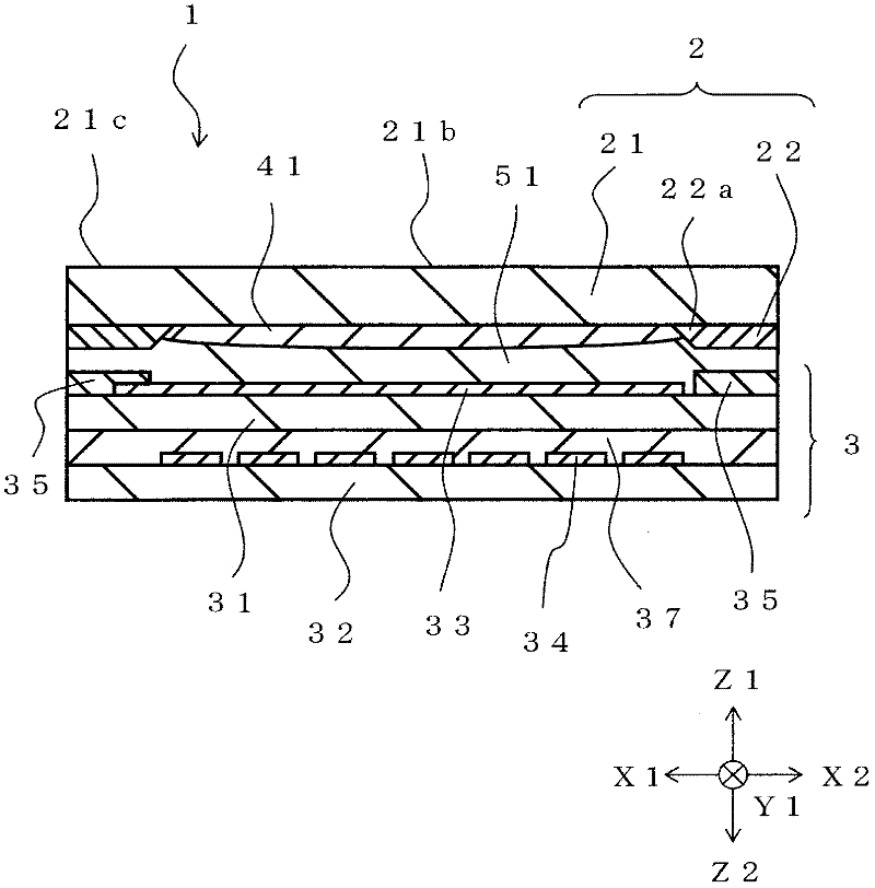
[0078] figure 1 It is a sectional view showing the input device 1 according to the first embodiment of the present invention. Such an input device 1 is mounted on a display unit of various electronic devices such as a portable device such as a mobile phone or a portable information terminal, a game device, a camera, and an imaging device in a state of being stacked and arranged on a display screen of a display device such as a liquid crystal panel. . The operator can see the image of the display device through the input device 1, and can directly touch various information displayed on the display screen with a finger or the like to perform an input operation.
[0079] Such as figure 1 As shown, the input device 1 is configured to have a sensor member 3 for detecting input position information and a protection member 2 for protecting the surface of the sensor member 3 . Furthermore, the sensor member 3 and the protective member 2 are bonded via the transparent filler 41 an...
no. 2 approach
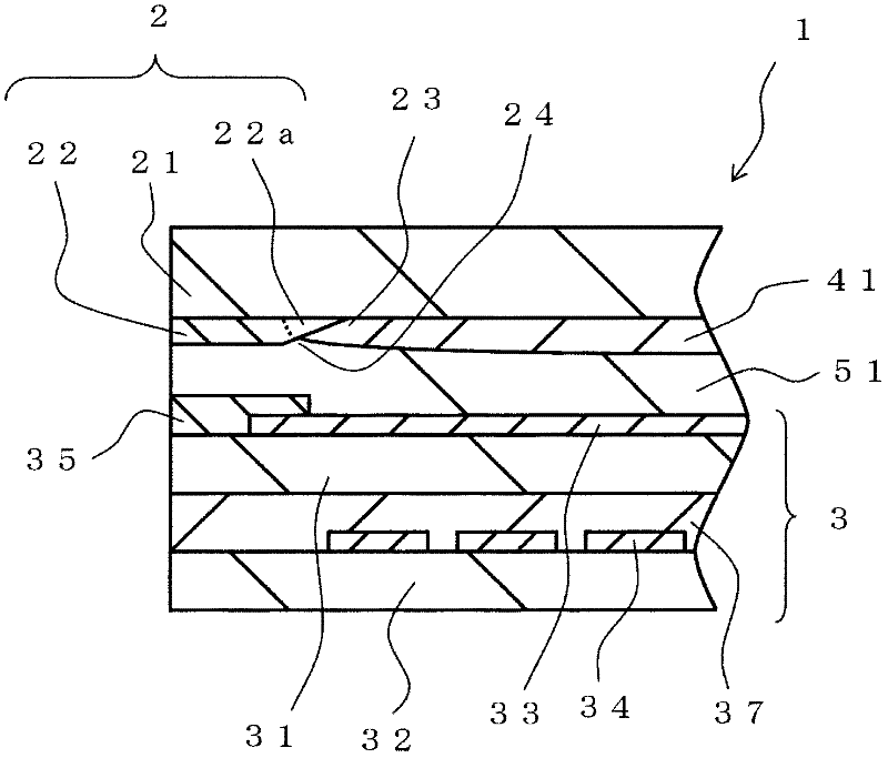
[0111] Figure 7 It is a sectional view showing the input device 1 of the second embodiment. In the input device 1 of the second embodiment, as in the first embodiment, the protective member 2 and the sensor member 3 are integrally bonded via the transparent filler 41 and the adhesive layer 51 , and the sensor member 3 constitutes a capacitive touch sensor.
[0112] In the second embodiment, the first wiring pattern 35 is formed on the outer peripheral portion of the first sensor base material 31 , and the protective layer 42 covering the upper portion of the first wiring pattern 35 is formed. In the input device 1, in order to enlarge the light-transmitting area 21b, it is required to further reduce the wiring of the first wiring pattern 35, thereby narrowing the non-light-transmitting area 21c. Therefore, a protective layer 42 is provided on the first wiring pattern 35 to prevent disconnection or short circuit. The protective layer 42 can be formed by using the same resin ...
no. 3 approach
[0116] Figure 8 It is a sectional view showing the input device 1 of the third embodiment. Such as Figure 8 As shown, the sensor member 3 of the third embodiment constitutes a resistive film type touch sensor. In the sensor member 3 of the present embodiment, the first sensor base material 31 and the second sensor base material 32 are arranged to face each other with a space provided therebetween with a spacer 38 interposed therebetween. In addition, a first electrode pattern 33 and a second electrode pattern 34 are respectively formed on the opposing surfaces of the first sensor base material 31 and the second sensor base material 32 .
[0117] The first sensor substrate 31 arranged on the input surface side is a flexible film-like material deformable according to an input operation, and transparent resin such as PET (polyethylene terephthalate) is used. The thickness of the first sensor substrate 31 is about 100 μm to 200 μm, for example, it is formed with a thickness o...
PUM
 Abstract
Description
Claims
Application Information
 - R&D Engineer
- R&D Manager
- IP Professional
- Industry Leading Data Capabilities
- Powerful AI technology
- Patent DNA Extraction
Browse by: Latest US Patents, China's latest patents, Technical Efficacy Thesaurus, Application Domain, Technology Topic, Popular Technical Reports.
© 2024 PatSnap. All rights reserved.Legal|Privacy policy|Modern Slavery Act Transparency Statement|Sitemap|About US| Contact US: help@patsnap.com