
Device monitoring method during semiconductor process

A device monitoring, semiconductor technology

Active Publication Date: 2013-12-04
SHANGHAI HUALI MICROELECTRONICS CORP
View PDF7 Cites 0 Cited by
  • Summary
  • Abstract
  • Description
  • Claims
  • Application Information

AI Technical Summary

Problems solved by technology

However, both of the above forms of monitoring have limitations and risk periods, thus creating uncertainty in production
Offline monitoring can only be carried out when the equipment is not in production, so that the monitoring frequency is low, and the uncertainty in production cannot be monitored in time
Online monitoring is a part of the whole process, but it is usually impossible to inspect all wafers. After the products arrive at the online inspection station, they are selected according to the defined sampling rules. Products that do not meet the sampling rules are automatically skipped to the next station without making defects. Inspection, and the selection of running equipment after the product arrives at the main process site is random, so it may cause that the products released by a certain main process equipment within a period of time have not been inspected for defects. Time out of monitoring and monitoring, so that the risk expands
The actual practice of traditional semiconductor factories is the above-mentioned sampling inspection, which leads them to bear the risk of a large number of wafers being skipped in production

Method used


Image

  • Device monitoring method during semiconductor process
  • Device monitoring method during semiconductor process
  • Device monitoring method during semiconductor process

Examples


Embodiment Construction

[0026] The present invention will be further described below in conjunction with the accompanying drawings and specific embodiments, but not as a limitation of the present invention.

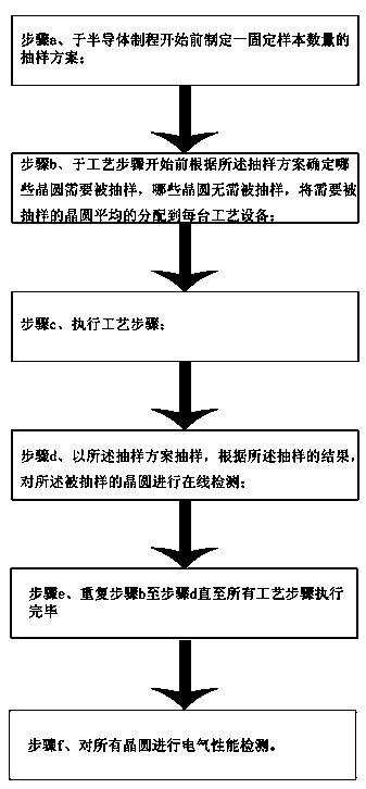
[0027] like figure 1 The device monitoring method in a semiconductor manufacturing process shown in the present invention includes the following steps:

[0028] Step a, formulating a sampling plan with a fixed number of samples before the start of the semiconductor manufacturing process;

[0029] Step b. Determine which wafers need to be sampled and which wafers do not need to be sampled according to the sampling plan before the start of the process steps, and evenly distribute the wafers that need to be sampled to each process equipment;

[0030] Step c, performing the process steps;

[0031] Step d, sampling with a sampling plan, and performing online detection on the sampled wafers according to the sampling results;

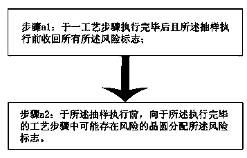
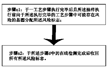
[0032] Step e, repeating step b to step d until all process steps are ex...


PUM


Abstract

The invention provides a method for monitoring devices in semiconductor process comprising: Step a, designing a sampling plan with fixed sample size before the beginning of the semiconductor process; Step b, determining whether to sample the wafers according to the sampling plan and dispatching the wafers to be sampled to each process device before the beginning of the process step, wherein the process device is used for performing the process step; Step c, performing the process step; Step d, sampling the wafers according to the sampling plan, and performing in-line inspection to the sampled wafers according to the sampling results; Step e, repeating Step b to Step d until all the process steps are completed; Step f, performing e-test to all the wafers. According to the method, the potential risk during the semiconductor process can be minimized through the coordination of the sampling plan and the dynamic risk flag.

Description

technical field [0001] The invention designs a monitoring method in the field of semiconductor manufacturing, in particular, an equipment monitoring method in a semiconductor manufacturing process that can improve product yield. Background technique [0002] The manufacture of semiconductor integrated circuits involves hundreds of process steps, and any one of these steps out of control may cause the final product to fail even if the other steps are well controlled. Therefore, monitoring each process step and having early warning is one of the key issues in the semiconductor integration process. [0003] Traditional semiconductor factories use two forms of monitoring, offline monitoring and online monitoring, to check the performance of equipment during operation. However, both of the above monitoring forms have limitations and risk periods, which bring uncertainty to production. Offline monitoring can only be carried out when the equipment is not in production, so that th...

Claims


Application Information

Patent Timeline
Patent Type & Authority Patents(China)
IPC IPC(8): H01L21/66
CPCH01L22/14H01L22/20H01L22/10
Inventor 陈宏璘王恺朱陆君倪棋梁龙吟郭明升
Owner SHANGHAI HUALI MICROELECTRONICS CORP
Learn More