
Pixel structure of organic light emitting diode (OLED)

A technology of light-emitting display and pixel structure, applied in the field of pixel structure, can solve the problems of deposition, masking difficulties, sub-pixel light color mixing, etc., and achieve the effects of prolonging service life, increasing resolution, and increasing aperture ratio

Inactive Publication Date: 2012-02-15
AU OPTRONICS CORP
View PDF0 Cites 20 Cited by
  • Summary
  • Abstract
  • Description
  • Claims
  • Application Information

AI Technical Summary

Problems solved by technology

The smaller the spacing between adjacent sub-pixels, the higher the resolution of the display panel, but it is easy to produce alignment errors during the manufacturing process, which will cause the color organic layer in the sub-pixel to be deposited into the adjacent sub-pixel, resulting in sub-pixel Color mixing occurs in the light emitted by the pixels
The arrangement of the sub-pixels will also make the corresponding mask encounter considerable difficulties in etching. Therefore, it is difficult to manufacture a high-resolution organic light-emitting display (abbreviated as OLED) using the existing sub-pixel arrangement.

Method used


Image

  • Pixel structure of organic light emitting diode (OLED)
  • Pixel structure of organic light emitting diode (OLED)
  • Pixel structure of organic light emitting diode (OLED)

Examples


Embodiment Construction

[0018] The specific implementation manners of the present invention will be described in further detail below with reference to the accompanying drawings.

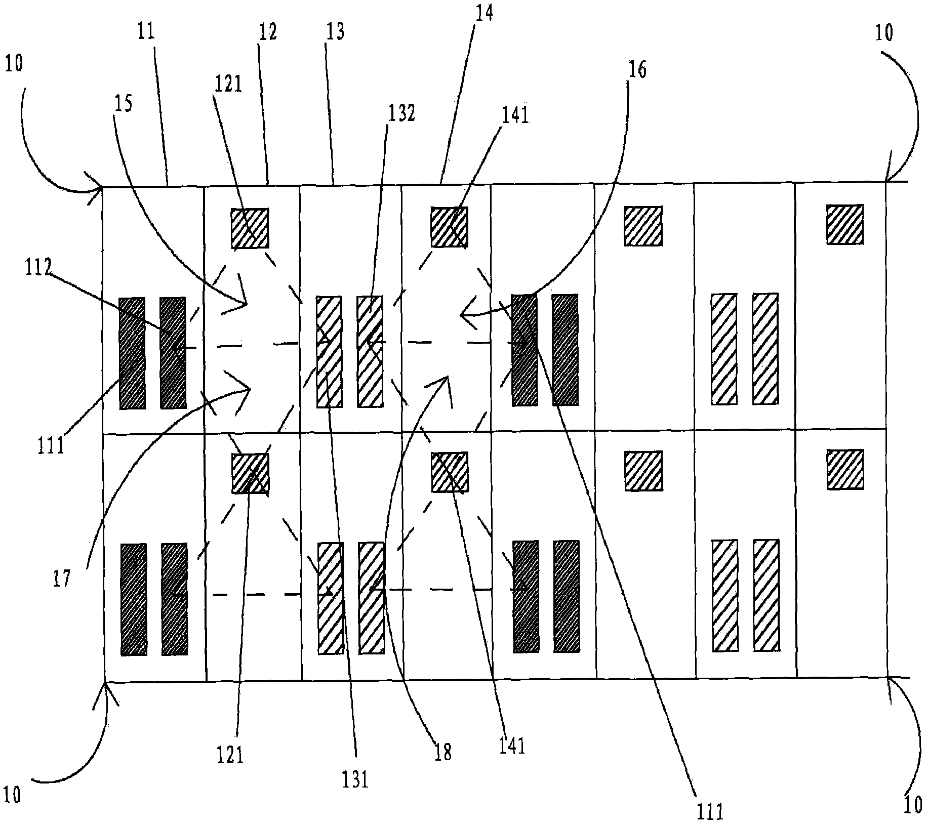
[0019] figure 1 A schematic diagram showing a pixel structure of an organic light emitting display according to an embodiment of the present invention. refer to figure 1 The pixel structure 1 is located on a substrate (not shown), and includes a plurality of pixels 10 arranged in a matrix along the X-axis direction and the Y-axis direction. Each pixel 10 includes a first sub-pixel 11, two second sub-pixels 12 and 14, and a third sub-pixel 13. In the X-axis direction, the first sub-pixel 11, the second sub-pixel 12, the second sub-pixel The three sub-pixels 13 and the second sub-pixel 14 are arranged in sequence. The first sub-pixel 11 has two first light-emitting regions 111 and 112 , the third sub-pixel 13 has two third light-emitting regions 131 and 132 , and the second sub-pixels 12 and 14 have a second light-emittin...


PUM


Abstract

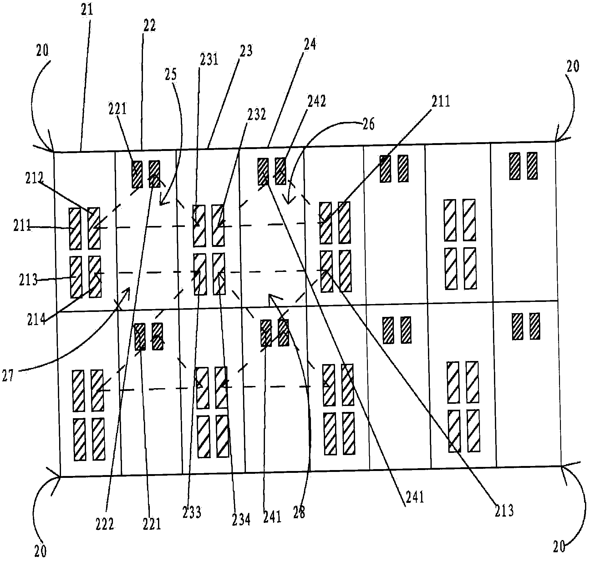
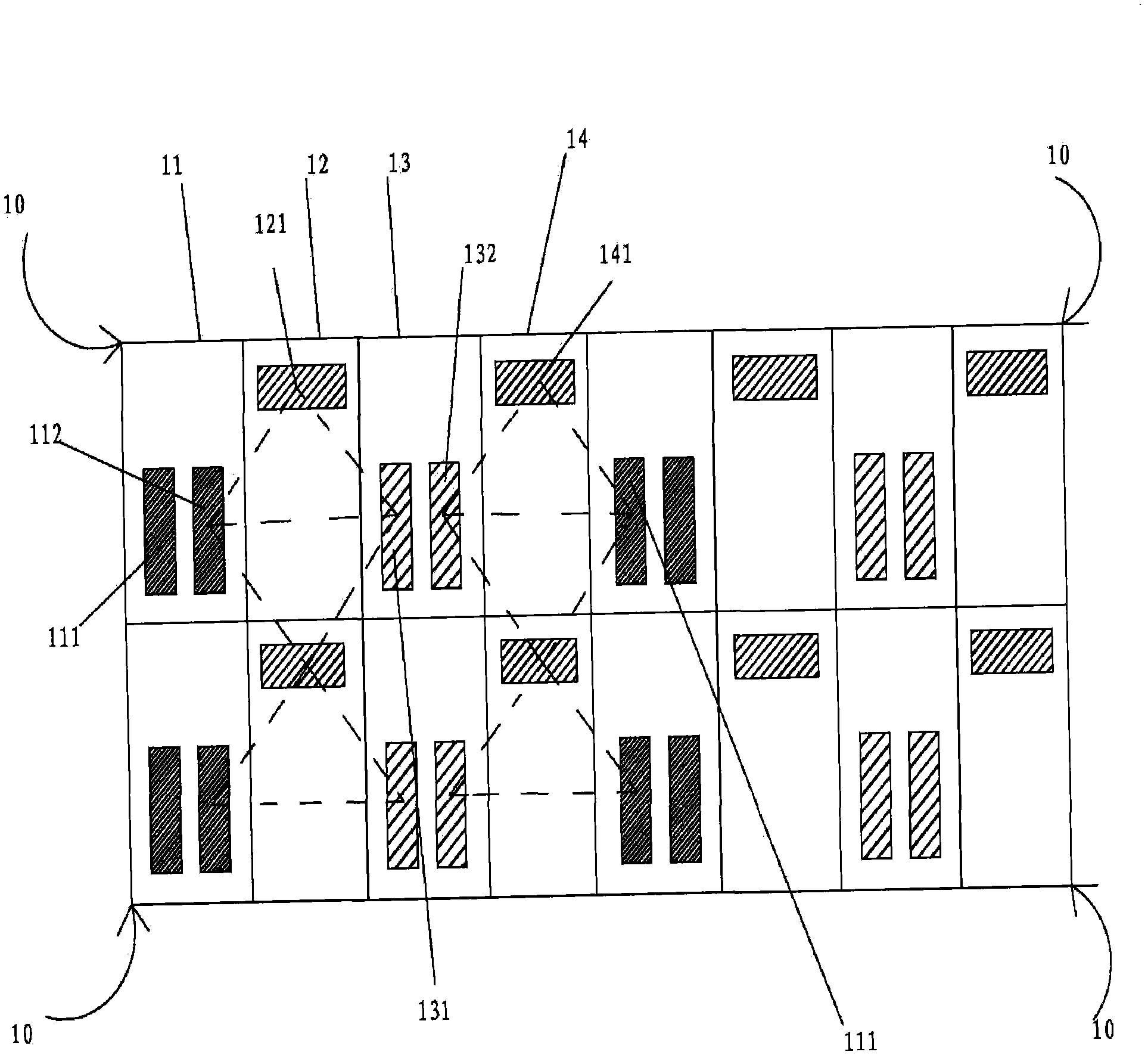
The invention provides a pixel structure of an organic light emitting diode (OLED). The pixel structure is arranged on a substrate and comprises a plurality of pixels, wherein the pixels are arranged in a matrix in the X-axis and Y-axis directions; each pixel comprises a first subpixel, two second subpixels and a third subpixel; the first subpixel, one second subpixel, the third subpixel and the other second subpixel are arranged in sequence in the X-axis direction; the first subpixel comprises two first light emitting zones; each second subpixel comprises a second light emitting zone; the third subpixel comprises two third light emitting zones; and the adjacent first light emitting zone, second light emitting zone and third light emitting zone are arranged in a triangle, the geometric centers of the three light emitting zones are arranged on different peaks of the triangle, and one side of the triangle formed by connecting the geometric centers of the first light emitting zone and the third light emitting zone, is parallel to the X-axis. The pixel structure has the following advantages: by adopting the pixel structure, color mixture can be avoided, the resolution can be increased and the aperture ratio can be increased and the service life can be prolonged.

Description

technical field [0001] The present invention relates to a pixel structure, in particular to a pixel structure of an organic light emitting display. Background technique [0002] Organic light-emitting display (organic light emitting diode, abbreviated as OLED) has a large viewing angle, excellent contrast and high response speed, and has the characteristics of thinness, power saving, high resolution, etc., and has become the mainstream flat panel display. It is considered to be a new generation of displays. [0003] The color image of an organic light emitting display (OLED for short) is mainly provided by a plurality of pixels, and these pixels have three sub-pixels of red, green and blue. The design of the pixel structure affects the resolution of an organic light emitting diode (OLED for short). In the prior art, in the display structure of an organic light-emitting display (abbreviated as OLED), each pixel has three sub-pixels of red, green and blue, and these three su...

Claims


Application Information

Patent Timeline
Patent Type & Authority Applications(China)
IPC IPC(8): H01L27/32
Inventor 陈宪泓徐士峰
Owner AU OPTRONICS CORP
Learn More