Longitudinally-conductive GaN (gallium nitride) normally-closed MISFET (metal integrated semiconductor field effect transistor) device and manufacturing method thereof
A manufacturing method and a normally-off technology, which is applied in the manufacture of semiconductor/solid-state devices, semiconductor devices, electrical components, etc., can solve the problem of reduced electron mobility in the channel, damage to the lattice at the edge of the groove, and increased on-resistance of the device etc. to achieve the effect of improving mobility, reducing on-resistance, and increasing threshold voltage
- Summary
- Abstract
- Description
- Claims
- Application Information
AI Technical Summary
Problems solved by technology
Method used
Image
Examples
Embodiment 1
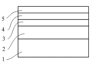
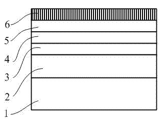
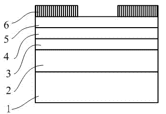
[0041] Such as Figure 10 Shown is a schematic diagram of the device structure of this embodiment, including a gate 11, a source 9, a drain 10, an insulating layer 8, a conductive GaN substrate 1, an n-type GaN layer 2, an electron blocking layer 3, and a non-doped GaN layer 4 and the heterostructure barrier layer 5, dry etching to form grooves, secondary growth of the p-type GaN layer to realize the gate conductive channel 7, the surface of the channel 7 and the heterostructure barrier layer 5 covering the insulating layer 8 , the gate 11 covers the channel 7 on the insulating layer, and the insulating layer 8 and SiO are etched 2 A source region is formed at both ends of the mask, and ohmic metal is evaporated on the source region to form a source 5 in contact with the heterostructure barrier layer 5, and the drain 10 is placed on the back of the conductive GaN substrate. In this embodiment, the conductive GaN substrate 1 is a heavily doped GaN substrate, and the n-type GaN...
Embodiment 2
[0054] Such as Figure 11 Shown is a schematic diagram of the device structure of this embodiment, which is similar to that of Embodiment 1, except that an AlN layer 12 with a thickness of 5-50 nm is grown on the electron blocking layer 3 before the non-doped GaN layer 4 is grown. Because in the growth of the electron blocking layer 3, in order to make this layer form a high-resistance blocking layer of electrons, p-type doping is carried out, and impurities may diffuse into the non-doped GaN layer 4 on the upper layer during the growth process, affecting device performance. Therefore, the introduction of a thin layer of AlN layer 12 will effectively block the diffusion of these impurities into the non-doped GaN layer 4 .
Embodiment 3
[0056] Such as Figure 12 Shown is a schematic diagram of the device structure of this embodiment, which is similar to the structure of Embodiment 1, the only difference is that the mask layer 6 is not removed after the groove is etched in the gate region, and the subsequent process steps are directly carried out. The purpose of doing this is to reduce the steps of removing the mask layer 6 and simplify the process flow, and at the same time, the mask layer 6 can be used as a passivation layer.
PUM
 Abstract
Description
Claims
Application Information
 - R&D Engineer
- R&D Manager
- IP Professional
- Industry Leading Data Capabilities
- Powerful AI technology
- Patent DNA Extraction
Browse by: Latest US Patents, China's latest patents, Technical Efficacy Thesaurus, Application Domain, Technology Topic, Popular Technical Reports.
© 2024 PatSnap. All rights reserved.Legal|Privacy policy|Modern Slavery Act Transparency Statement|Sitemap|About US| Contact US: help@patsnap.com


