Method of electron diffraction tomography
A technology of electron diffraction and tomography, applied in material analysis using radiation diffraction, material analysis using wave/particle radiation, circuits, etc., can solve problems such as small interactions
- Summary
- Abstract
- Description
- Claims
- Application Information
AI Technical Summary
Problems solved by technology
Method used
Image
Examples
Embodiment Construction
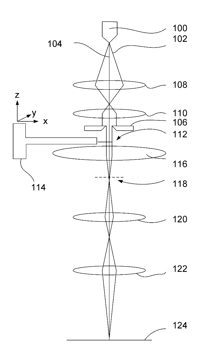
[0067] figure 1 The optical elements of a TEM for carrying out the method according to the invention are schematically shown.
[0068] figure 1 An electron source 100 is shown for generating an energetic electron beam 102 along an electron-optical axis 104 , for example with an energy of 50 to 400 keV.
[0069] Note that in reality, the location where the beam is focused (crossovers shown) is different from where it is drawn - and thus the angle and linear magnification are different, but these intersections are used to limit the beam diameter.
[0070] Note also that electron microscopes using lower and higher beam energies are known. Note that there may be one or more lenses located between the electron source and the aperture as well as alignment coils to center the beam on-axis. Condenser lenses 108 and 110 are used to form a beam at a sample position 112 . The diameter of the beam at the sample location is governed by the aperture 106 . The sample is placed on said s...
PUM
| Property | Measurement | Unit |
|---|---|---|
| diameter | aaaaa | aaaaa |
| diameter | aaaaa | aaaaa |
| size | aaaaa | aaaaa |
Abstract
Description
Claims
Application Information
 - R&D
- Intellectual Property
- Life Sciences
- Materials
- Tech Scout
- Unparalleled Data Quality
- Higher Quality Content
- 60% Fewer Hallucinations
Browse by: Latest US Patents, China's latest patents, Technical Efficacy Thesaurus, Application Domain, Technology Topic, Popular Technical Reports.
© 2025 PatSnap. All rights reserved.Legal|Privacy policy|Modern Slavery Act Transparency Statement|Sitemap|About US| Contact US: help@patsnap.com


