Method for preparing semiconductor substrate with insulating buried layer and semiconductor substrate

An insulating buried layer, semiconductor technology, used in semiconductor devices, semiconductor/solid-state device manufacturing, electrical components and other directions, can solve problems such as low device yield, achieve perfect lattice, no primary defects, low oxygen and metal content Effect

Inactive Publication Date: 2011-12-28
SHANGHAI SIMGUI TECH +1
View PDF3 Cites 7 Cited by
  • Summary
  • Abstract
  • Description
  • Claims
  • Application Information

AI Technical Summary

Problems solved by technology

[0003] However, for SOI materials, due to the existence of the buried oxide layer, there is no DZ region in the top layer of silicon, which makes the yield of SOI devices relatively low

Method used


Image

  • Method for preparing semiconductor substrate with insulating buried layer and semiconductor substrate
  • Method for preparing semiconductor substrate with insulating buried layer and semiconductor substrate
  • Method for preparing semiconductor substrate with insulating buried layer and semiconductor substrate

Examples


Embodiment Construction

[0014] Next, a method for preparing a semiconductor substrate with an insulating buried layer and specific implementations of the semiconductor substrate according to the present invention will be described in detail with reference to the accompanying drawings.

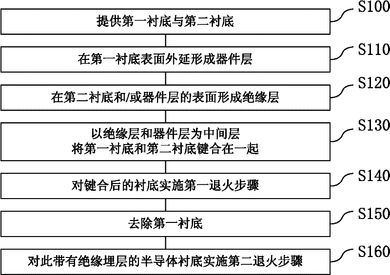
[0015] attached figure 1 Shown is a schematic diagram of the implementation steps of the method described in the specific embodiment of the present invention, including: step S100, providing a first substrate and a second substrate; step S110, epitaxially forming a device layer on the surface of the first substrate; step S120, in An insulating layer is formed on the surface of the second substrate and / or the device layer; Step S130, using the insulating layer and the device layer as an intermediate layer, bonding the first substrate and the second substrate together; Step S140, after bonding The substrate implements the first annealing step; Step S150, removes the first substrate to form a semiconductor substrate with...


PUM


Abstract

A method for preparing a semiconductor substrate with an insulating buried layer, comprising the steps of: providing a first substrate and a second substrate; epitaxially forming a device layer on the surface of the first substrate; An insulating layer is formed on the surface of the layer; the first substrate and the second substrate are bonded together with the insulating layer and the device layer as the intermediate layer; the first annealing step is performed on the bonded substrate; the first substrate is removed , forming a semiconductor substrate with an insulating buried layer consisting of a device layer, an insulating layer and a second substrate; implementing a second annealing step on the semiconductor substrate with an insulating buried layer, the annealing of the second annealing step The temperature is greater than the annealing temperature of the first annealing step. The advantage of the present invention is that the obtained SOI material top layer silicon is completely composed of epitaxial materials. Compared with the SOI material top layer semiconductor layer produced by conventional processes, its oxygen element and metal content are lower, and the crystal lattice is perfect, no native defects are generated, and it can be greatly improved. Significantly improve the yield of the device.

Description

technical field [0001] The invention relates to a method for preparing a silicon-on-insulator material, in particular to a method for preparing a semiconductor substrate with an insulating buried layer and the semiconductor substrate. Background technique [0002] Control of defects in silicon single crystals becomes especially important as the feature size of integrated circuits decreases. Defects in silicon wafers mainly come from two aspects. On the one hand, the original defects generated during the crystal growth process, such as crystal primary particles (COPs); on the other hand, defects generated during the heat treatment of silicon wafers, such as oxygen precipitation, these defects If it is in the active area on the surface of the silicon wafer, it will have a damaging effect on the performance of the device and cause the device to fail. In addition, silicon wafers are inevitably contaminated by metals such as Cu, Ni, and Fe during processing and integrated circui...

Claims


Application Information

Patent Timeline
Patent Type & Authority Applications(China)
IPC IPC(8): H01L21/762H01L21/20H01L29/06
Inventor 魏星仰庶曹共柏张峰王曦
Owner SHANGHAI SIMGUI TECH
Why Eureka
Try Eureka