GaN-based laser and method for measuring AlGaN/GaN superlattice resistivity

A laser and superlattice technology, applied in lasers, laser components, semiconductor lasers, etc., can solve problems such as limiting the development of GaN-based laser technology, large impact differences, and difficulty in optimizing AlGaN/GaN superlattice structures

Inactive Publication Date: 2013-04-17
BEIJING UNIV OF CHEM TECH
View PDF2 Cites 0 Cited by
  • Summary
  • Abstract
  • Description
  • Claims
  • Application Information

AI Technical Summary

Problems solved by technology

Due to the high ionization energy of acceptor impurities in P-type AlGaN, the hole concentration of the P-type AlGaN optical confinement layer in GaN-based lasers is relatively low, which makes the resistivity of the p-type part of the laser relatively high, resulting in high operating voltage of the laser.
The use of AlGaN / GaN superlattice can reduce the working voltage, but the influence of different structures of AlGaN / GaN superlattice as the optical confinement layer on the working voltage of GaN-based lasers is quite different
Due to the complexity of GaN-based laser structure and manufacturing process, it is difficult to confirm the direct relationship between the change of a certain laser operating voltage and the adoption of AlGaN / GaN superlattice, which brings a lot to the structural optimization of AlGaN / GaN superlattice. Difficulties, limiting the development of GaN-based laser technology

Method used


Image

  • GaN-based laser and method for measuring AlGaN/GaN superlattice resistivity
  • GaN-based laser and method for measuring AlGaN/GaN superlattice resistivity
  • GaN-based laser and method for measuring AlGaN/GaN superlattice resistivity

Examples


Embodiment 1

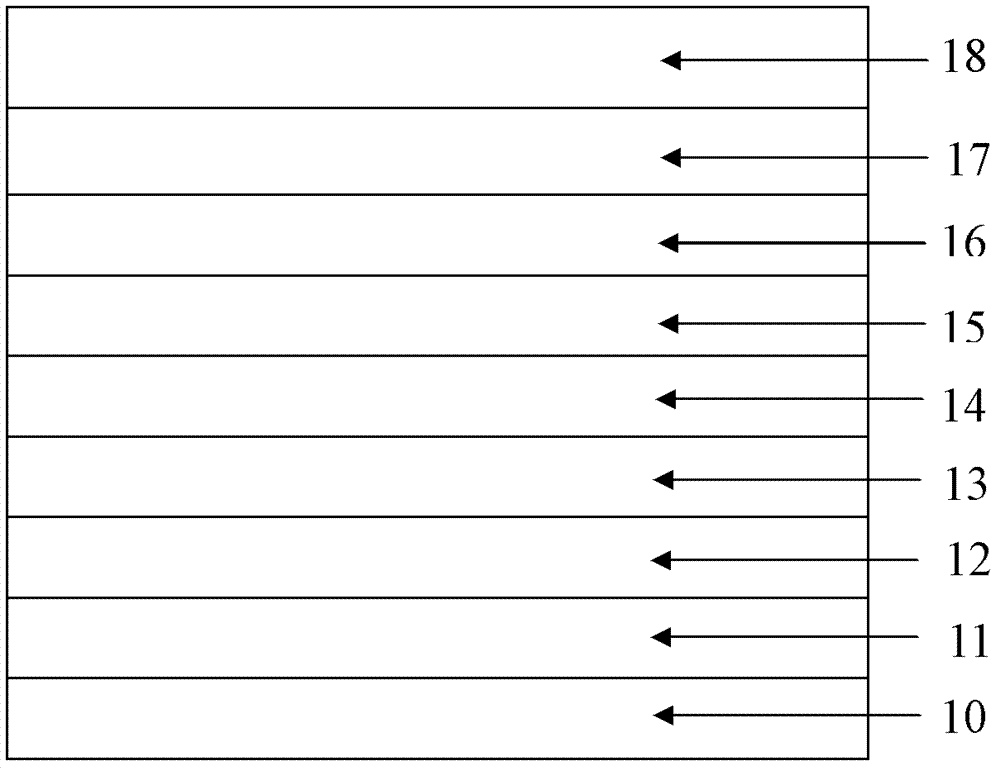
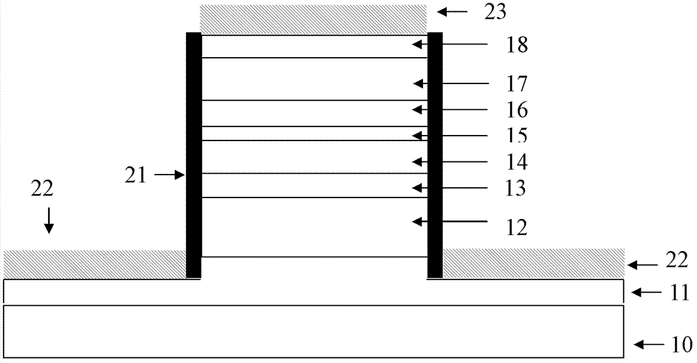
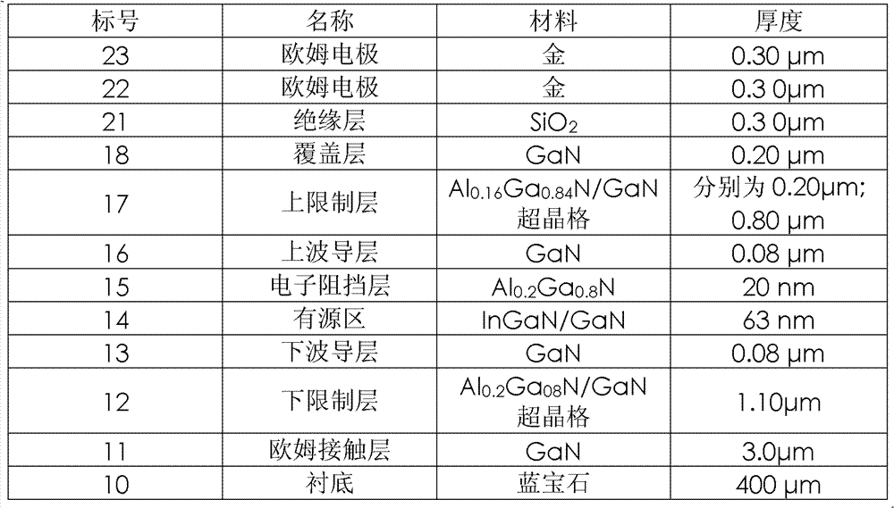
[0075] In order to further illustrate the effect of the device structure, we take a GaN-based laser with an operating wavelength of 405nm as an example to illustrate the preparation process of the device structure. The material and thickness of each layer are shown in Table 1. The details are as follows: the device structure is grown on the (0001) plane sapphire substrate 10 by MOCVD method. The structure includes an n-type ohmic contact layer 11 (thickness is 3.0 μm, doping concentration is 6.5×10 15 cm -3 ), n-type Al 0.2 Ga 0.8 N / GaN superlattice lower confinement layer 12 (thickness is 1.10 μ m, GaN well width is 2.0 nm, Al 0.2 Ga 0.8 N barrier width is 2.0nm, doping concentration is 3.0×10 18 cm -3 ), n-type GaN lower waveguide layer 13 (thickness is 0.08 μm, doping concentration is 5.0×10 15 cm -3 ), In 0.15 Ga 0.85 N / GaN active region layer 14 (multiple quantum wells are 5 periods, InGaN well width is 3nm, GaN barrier width is 8nm, doping concentration is 3.0...

Embodiment 2

[0078] In order to further illustrate the effect of the device structure, we take a GaN-based laser with an operating wavelength of 405nm as an example to illustrate the preparation process of the device structure. The material and thickness of each layer are shown in Table 2. The details are as follows: the device structure is grown on the (0001) plane sapphire substrate 10 by MOCVD method. The structure includes an n-type ohmic contact layer 11 (thickness is 3.0 μm, doping concentration is 6.5×10 15 cm -3 ), n-type Al 0.2 Ga 0.8 N / GaN superlattice lower confinement layer 12 (thicknesses of the layers in the two epitaxial wafers are 0.3 μm and 1.1 μm respectively, Ga N well width is 2.0 nm, Al 0.2 Ga 0.8 N barrier width is 2.0nm, doping concentration is 3.0×10 18 cm -3 ), n-type GaN lower waveguide layer 13 (thickness is 0.08 μm, doping concentration is 5.0×10 15 cm -3 ), In 0.15 Ga 0.85 N / GaN active region layer 14 (multiple quantum wells are 5 periods, InGaN well...


PUM


Abstract

The invention relates to a laser structure and a method for measuring AlGaN / GaN superlattice resistivity in a GaN-based semiconductor laser. The laser for measuring the optical confinement layer resistivity of AlGaN / GaN superlattice is divided into two types of lasers with an n-type or p-type AlGaN / GaN superlattice optical confinement layers of different thicknesses; the serial resistance of eachtype of laser is determined through measuring the I-V (current / voltage) characteristic curve of the laser; the difference of the serial resistance of the laser for the AlGaN / GaN superlattice optical confinement layers of different thicknesses is the resistance of the AlGaN / GaN superlattice of changed thicknesses, thus the resistivity of the AlGaN / GaN superlattice optical confinement layers can beobtained. Through utilizing the laser with the structure, the resistivity of the n-type and p-type AlGaN / GaN superlattice optical confinement layers in the GaN-based semiconductor laser can be measured respectively, and reference data is provided for the structural design and development manufacturing of the GaN-based semiconductor laser.

Description

technical field [0001] The invention belongs to the field of semiconductor devices, in particular to a GaN-based semiconductor laser used for measuring the resistivity of AlGaN / GaN superlattice and its manufacturing and testing methods. Background technique [0002] As a third-generation semiconductor, gallium nitride (GaN) and its series of materials (including aluminum nitride, aluminum gallium nitride, indium gallium nitride, and indium nitride) are characterized by their large band gap and wide spectral range (covering from ultraviolet to Infrared full band), high temperature resistance and corrosion resistance, it has great application value in the field of optoelectronics and microelectronics. GaN-based lasers are very important GaN-based optoelectronic devices. Because the light waves emitted by them are in the blue-violet light band, GaN-based lasers are used in high-density optical information storage, projection display, laser printing, underwater communication, ac...

Claims


Application Information

Patent Timeline
Patent Type & Authority Patents(China)
IPC IPC(8): H01S5/343H01S5/22H01S5/042H01S5/00
Inventor 李德尧许海军吴超廛宇飞朱建军赵德刚张书明杨辉
Owner BEIJING UNIV OF CHEM TECH
Why Eureka
Try Eureka