
Wafer processing apparatus having a tunable electrical resistivity

A technology of resistivity and volume resistivity, which is applied in the manufacture of circuits, electrical components, semiconductors/solid-state devices, etc., can solve problems such as limiting the usable temperature range of wafer heating devices and reducing the resistance of halogen plasmas

Inactive Publication Date: 2011-09-28
MOMENTIVE PERFORMANCE MATERIALS INC
View PDF21 Cites 4 Cited by
  • Summary
  • Abstract
  • Description
  • Claims
  • Application Information

AI Technical Summary

Problems solved by technology

This leakage current limits the usable temperature range of the wafer heater
AlN films can be replaced by materials with higher resistivity, however, the resistance to halogen plasma may be reduced

Method used


Image

  • Wafer processing apparatus having a tunable electrical resistivity
  • Wafer processing apparatus having a tunable electrical resistivity
  • Wafer processing apparatus having a tunable electrical resistivity

Examples


Embodiment

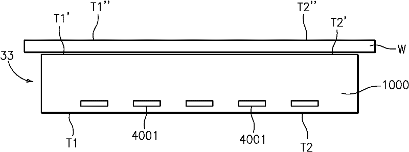
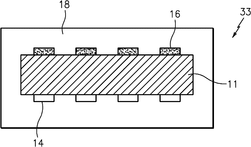
[0060] Examples of layered AlN are shown in Table 1 and Figure 8 . This example utilizes 3 types of AlN films with different resistivities. Type A AlN is a low-density low-resistivity film; Type B AlN is a high-density mid-range resistivity film; and Type C AlN is an ultra-high resistivity AlN film. The measured 600°C resistivity of each type of AlN is shown in Table 1. Sample 70858 consists of 3 layers of AlN, where the 1st and 3rd layers are type A AlN and the 2nd layer is type B AlN. In this example, the composite resistivity of the three-layer coating falls between those of the individual layers, and the resistivity can be adjusted to 1.5 × 10 by controlling the thickness of the individual layers 7 ohm-cm. Sample 80153 is a double-layer structure, in which the resistivity is changed from 1.3×10 10 ohm-cm (only with AlN type C) tuned to 4.1×10 9 ohm-cm. A third example is provided to illustrate a three-layer structure using AlN of type B and type C, wherein the comp...


PUM

PropertyMeasurementUnit
crystal densityaaaaaaaaaa

Abstract

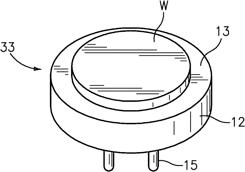
An article with an etch resistant coating is disclosed. The article is a heating element, wafer carrier, or electrostatic chuck. The article has a base substrate made of a ceramic or other material, and further has one or more electrodes for resistance heating or electromagnetic chucking or both. The eth resistant coating has a plurality of regions made from materials having different electrical volume resistivities, such that the overall coating has a bulk resistivity that can be tailored by varying the relative size of each region.

Description

Background technique [0001] Embodiments of the present invention generally relate to apparatus primarily for use in semiconductor wafer processing equipment on which an aluminum nitride coating is provided. More specifically, various embodiments relate to heating devices, wafer carriers, and electrostatic chucks having multiple regions of different resistivities on which coatings are applied. [0002] In one application, the wafer processing apparatus is particularly useful as a thermal electrostatic chuck for applications requiring heating of a semiconductor wafer from 100°C to 600°C while being electrostatically clamped to the surface of the thermal chuck. When the resistivity of the layer between the chuck electrode and the wafer falls within the Johnson-Rahbeck regime (regime) (see Figure 7 ) to obtain clamping force within the limited range. The invention enables the volume resistivity of the layer to be tuned to fall within the Johnson-Rahbeck specification at a given ...

Claims


Application Information

Patent Timeline
Patent Type & Authority Applications(China)
IPC IPC(8): H01L21/683
CPCH01L21/6831H01L21/683H01L21/6833
Inventor 戴维·M·鲁辛科马克·谢普肯斯曾万学
Owner MOMENTIVE PERFORMANCE MATERIALS INC
Learn More