
Processing method of circuit board and circuit board with contour tolerance of +/-0.05mm

A processing method and circuit board technology, applied in the directions of printed circuits, printed circuit manufacturing, electrical components, etc., can solve problems such as the inability to meet the external tolerances of circuit boards, to ensure continuity and consistency, prolong service life, and easy to obtain materials. Effect

Inactive Publication Date: 2012-12-19
大连亚太电子有限公司
View PDF0 Cites 0 Cited by
  • Summary
  • Abstract
  • Description
  • Claims
  • Application Information

AI Technical Summary

Problems solved by technology

[0005] The problems existing in the use of conventional processing methods on CNC drilling machines have been unable to meet the tolerance of the processed circuit boards within ±0.05mm

Method used


Image

  • Processing method of circuit board and circuit board with contour tolerance of +/-0.05mm
  • Processing method of circuit board and circuit board with contour tolerance of +/-0.05mm
  • Processing method of circuit board and circuit board with contour tolerance of +/-0.05mm

Examples


Embodiment Construction

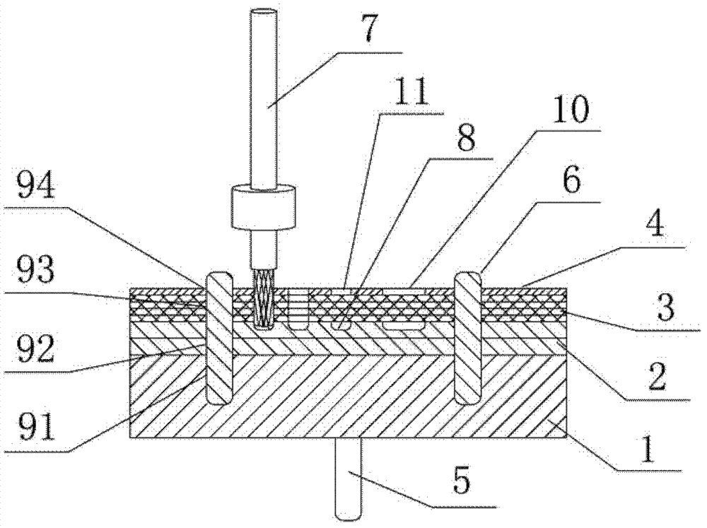
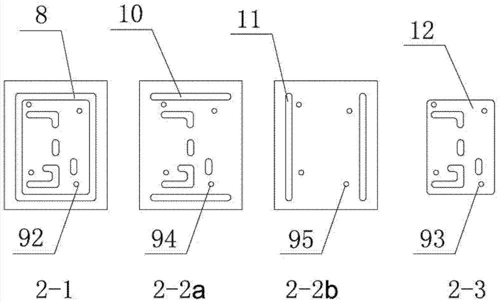
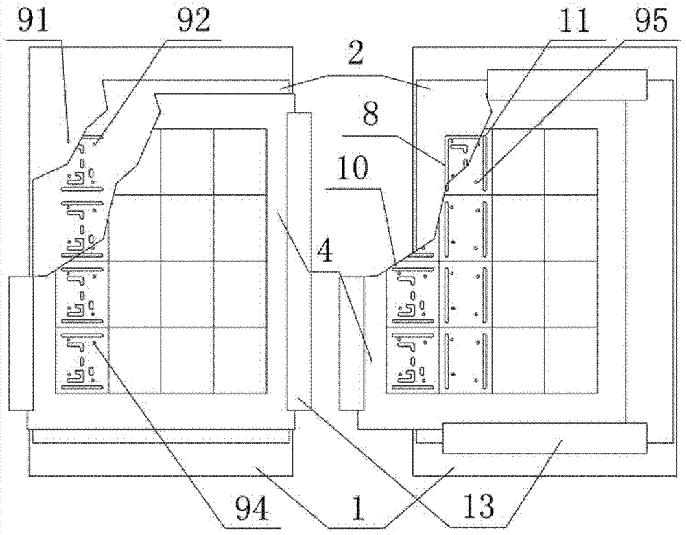
[0036] Such as Figure 1 to Figure 6 A processing method of a circuit board and a circuit board with a shape tolerance of ±0.05mm are shown. Paste an epoxy resin board with a vacuum channel on a special bakelite board as a backing board. The circuit board is placed on the pins that meet the tolerance requirements. There are at least three pins in the finished SET of each circuit board. Cover the circuit board with tape For the cover plate with milling slots, use a fixed row of pins on the bakelite board, and use a new milling cutter to perform two cycles of milling in the horizontal direction and the vertical direction for each row of the circuit board. Bakelite board: choose the bakelite board made of phenolic resin commonly used in the current circuit board production process, with a thickness of 10mm, and use two pins to fix it in the "one hole and one slot" positioning device on the milling machine table. Epoxy resin board: The ordinary prepreg used in circuit board manuf...


PUM

PropertyMeasurementUnit
thicknessaaaaaaaaaa
heightaaaaaaaaaa

Abstract

The invention discloses a processing method of a circuit board and a circuit board with a contour tolerance of + / -0.05mm. The processing method comprises the following steps: 1) fixing a special carte on a milling machine table top; 2) aligning and overlaying an epoxy resin board and a cover board on the special carte; 3) drilling a special carte dowel hole on the special carte, an epoxy resin board dowel hole on the epoxy resin board and the first row of dowel hole of the cover board; 4) processing the circulation milling path of the cover board and the epoxy resin board, which corresponds to the circuit board; 5) drilling the second row of dowel hole of the cover board; 6) putting a circuit board dowel on the epoxy resin board dowel hole on the epoxy resin board; 7) processing a millingcutter according to the first circulation milling flute and the second circulation milling flute of the cover board; and 8) processing the other rows of the circuit board according to the technology of step 7 to form the circuit board with contour tolerance of + / -0.05mm. The method is characterized in that precision can not be affected by external factors, the circuit board can be reused, and thecontinuity and the consistency of contour dimensional accuracy can be guaranteed.

Description

technical field [0001] The invention relates to a processing method of a circuit board and a circuit board with an appearance tolerance of ±0.05mm. Background technique [0002] In a sense, the history of electronics in recent decades can be seen as a history of gradual miniaturization. The main driving force for the transition to miniaturization of electronic products is the miniaturization of components and integrated circuits, and for packaging carriers- The requirements for processing dimensional tolerances of printed circuit boards are also increasing day by day. For example, the mobile phone board order of Dachang Electronics Co., Ltd. in Japan, etc., the tolerance requirement of the outer dimension of the finished board has reached ±0.05mm, which is a severe challenge for the printed board manufacturer. The reasons are as follows: [0003] At present, the commonly used circuit board CNC milling machine processing mode is: bakelite board + paper backing board + circui...

Claims


Application Information

Patent Timeline
Patent Type & Authority Patents(China)
IPC IPC(8): H05K3/00B23P17/00
Inventor 李景晓王大伟郑威曲键
Owner 大连亚太电子有限公司
Learn More