Method for manufacturing silicon-penetrating coaxial line for microwave frequency band

A technology of microwave frequency band and coaxial line, which is applied in the field of high-density packaging, can solve the problems of lithography ability and lithography precision limitation, coaxial line difficulty, etc., and achieve small mechanical and physical damage, smooth inner wall of through hole, and excellent process technology. Effects in simple steps

Inactive Publication Date: 2015-04-22
SHANGHAI INST OF MICROSYSTEM & INFORMATION TECH CHINESE ACAD OF SCI
View PDF3 Cites 0 Cited by
  • Summary
  • Abstract
  • Description
  • Claims
  • Application Information

AI Technical Summary

Problems solved by technology

However, this method is limited by the lithographic ability and lithographic accuracy of thick film materials, and it is difficult to prepare coaxial lines with high aspect ratios.

Method used


Image

  • Method for manufacturing silicon-penetrating coaxial line for microwave frequency band
  • Method for manufacturing silicon-penetrating coaxial line for microwave frequency band
  • Method for manufacturing silicon-penetrating coaxial line for microwave frequency band

Examples


Embodiment Construction

[0024] Embodiments of the present invention will be further specifically described below with reference to the accompanying drawings (6×6 array) in order to fully demonstrate the advantages and positive effects of the present invention. The scope of the present invention is not limited to the following examples.

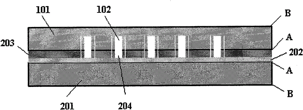
[0025] exist figure 1 In the example, on the A-side of the silicon wafer "1" 101, a 6×6 array of coaxial lines is distributed, and the coaxial line holes 102 are formed by a deep reactive ion etching (DRIE) process.

[0026] exist figure 2 In the above, the photosensitive BCB layer 203 is coated on the A side of the silicon wafer "2" 201, and the coaxial line pattern 204 is formed after photolithography.

[0027] image 3 The structure of the coaxial line 301 passing through the silicon wafer "1" 101 is formed after all processes such as bonding, electroplating and polishing are completed.

[0028] Figure 4-1 to Figure 4-6 It is a process flow of high-density ...


PUM


Abstract

The invention relates to a method for manufacturing a silicon-penetrating coaxial line for a microwave frequency band. The method is characterized by comprising the following steps of: photoetching a coaxial line pattern on an oxide layer at the A side of a silicon slice (1) and etching coaxial line through holes by using a deep reactive plasma etching process, wherein the depth of each coaxial line through hole is smaller than the thickness of the silicon slice; sputtering a seed layer on the A side of a silicon slice (2), covering a layer of photoconductive BCB (Benzocyclobutene) and photoetching to obtain the plated pattern of the coaxial line; then, aligning the A sides of the silicon slices (1 and 2) by using a BCB linkage process and linking at a low temperature; grinding the B side of the silicon slice (1) by using a chemical mechanical polishing process until through holes are exposed, and plating the coaxial line; and finally, grinding the silicon slice (2) from the B side to remove metal on the seed layer. By adopting wafer-level processes compatible with a microelectronics process, such as photoetching, and the like, the invention ensures the accuracy of a transmission line and can realize the mass manufacture. The silicon-penetrating coaxial transmission line lessens the influence on the microwave performance when a signal passes by the silicon slice in high-density three-dimensional encapsulation and avoids the great loss of the silicon-penetrating transmission line.

Description

technical field [0001] The invention relates to a method for manufacturing a through-silicon coaxial cable used in a microwave frequency band, and belongs to the field of high-density packaging. Background technique [0002] Coaxial line (Coaxial line) is a common signal transmission line. It is a transmission line composed of two coaxial cylindrical conductors. The core in the center transmits high level and is covered by insulating medium; The cylindrical metal layer of the shaft transmits low levels and at the same time acts as a shield. It is not only a double-conductor transmission line, which can transmit TEM waves, but also a coaxial cylindrical waveguide, which can transmit TE waves and TM waves. The TEM wave is the fundamental mode, and the TE and TM waves are high-order modes. The coaxial line works with TEM wave, has broadband characteristics, and can be used from DC to millimeter wave band. [0003] In order to realize high-density three-dimensional vertical pa...

Claims


Application Information

Patent Timeline
Patent Type & Authority Patents(China)
IPC IPC(8): H01P11/00H01L21/768H01P3/06
Inventor 汤佳杰罗乐徐高卫袁媛
Owner SHANGHAI INST OF MICROSYSTEM & INFORMATION TECH CHINESE ACAD OF SCI
Why Eureka
Try Eureka