Chip erasing method
A chip and word line technology, applied in the field of chip erasing in flash memory devices, can solve problems such as high power consumption, achieve the effects of reduced instantaneous power consumption, balanced decoding effect, and easy operation
- Summary
- Abstract
- Description
- Claims
- Application Information
AI Technical Summary
Problems solved by technology
Method used
Image
Examples
Embodiment approach
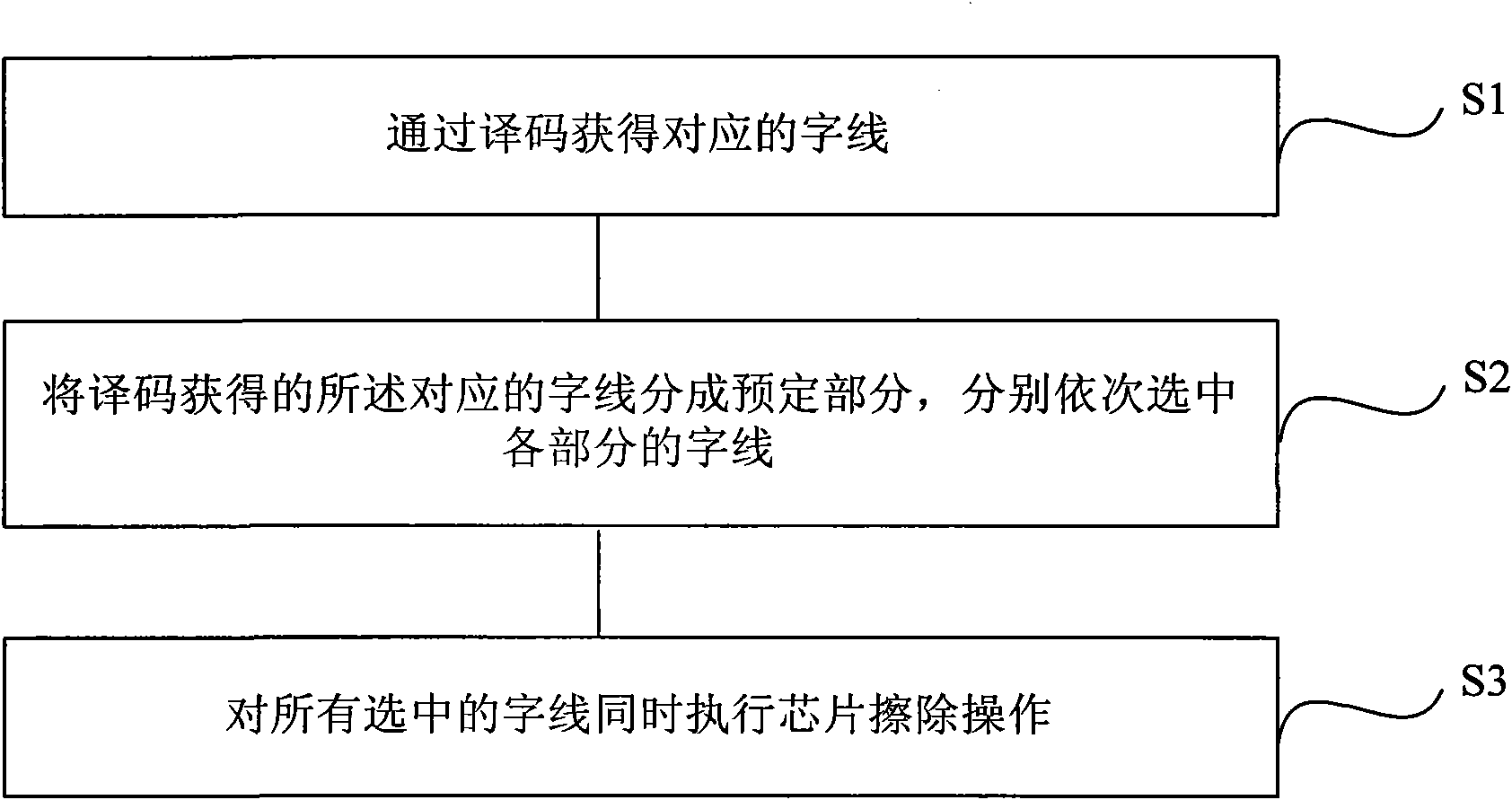
[0020] refer to image 3 , an implementation manner of the chip erasing method of the present invention may include:
[0021] Step S1, obtaining the corresponding word line through decoding;
[0022] Step S2, dividing the corresponding word lines obtained by decoding into predetermined parts, and sequentially selecting the word lines of each part;
[0023] In step S3, after the decoding of all word lines is completed, a chip erasing operation is performed.
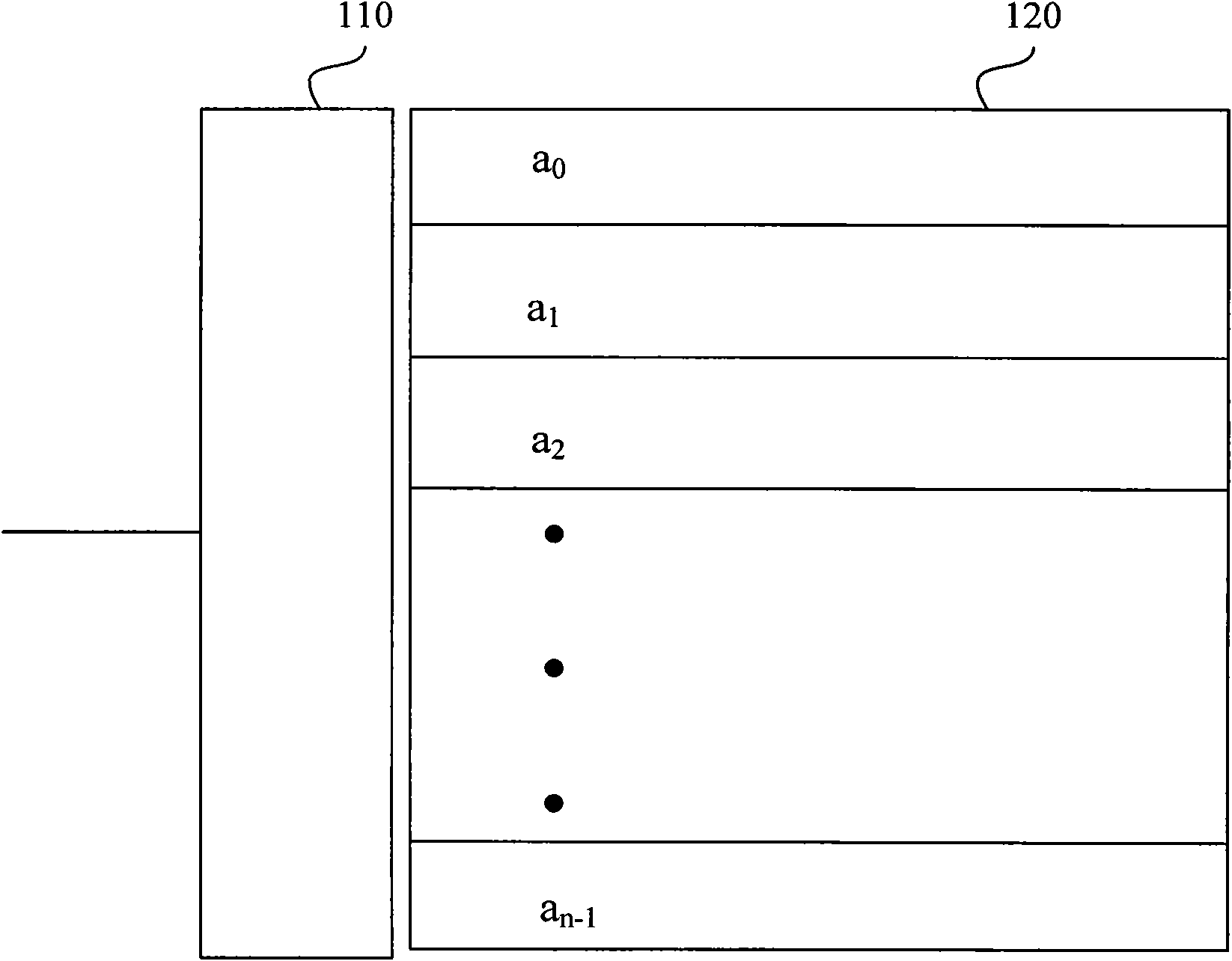
[0024] Wherein, the decoding method adopted in step S1 can be a bit-by-bit decoding mode, for example, according to the value of each word bit to determine the corresponding word line, for the 8-bit bit line (respectively a 7 a 6 a 5 a 4 a 3 a 2 a 1 a 0 ) decoder, its decoding result can correspond to 2 8 word lines, wherein the value of the bit line of the decoder corresponding to the decoding result of the 35th word line is 00100011. In addition, the decoding in step S1 may also include other decoding methods,...
PUM
 Abstract
Description
Claims
Application Information
 - R&D
- Intellectual Property
- Life Sciences
- Materials
- Tech Scout
- Unparalleled Data Quality
- Higher Quality Content
- 60% Fewer Hallucinations
Browse by: Latest US Patents, China's latest patents, Technical Efficacy Thesaurus, Application Domain, Technology Topic, Popular Technical Reports.
© 2025 PatSnap. All rights reserved.Legal|Privacy policy|Modern Slavery Act Transparency Statement|Sitemap|About US| Contact US: help@patsnap.com


