
Over-voltage protection element

A technology for protecting components and overvoltage, applied in the direction of overvoltage protection resistors, varistors, etc., can solve the problems of electrode short circuit, complicated steps, and high process difficulty.

Inactive Publication Date: 2010-08-18
THINKING ELECTRONIC IND CO LTD
View PDF1 Cites 2 Cited by
  • Summary
  • Abstract
  • Description
  • Claims
  • Application Information

AI Technical Summary

Problems solved by technology

[0009] see again Figure 8 As shown, however, when cutting the electrode layer 72 in the manufacturing method of the aforementioned voltage protection element, it is very easy to produce a burr 721 at the cutting place of the electrode layer 72. If the burr 721 is not handled properly, it is very easy to cause a short circuit of the electrode or still have a tip. The discharge situation exists. Therefore, the process steps of the overvoltage protection element are relatively complicated, time-consuming, and the process is difficult.

Method used


Image

  • Over-voltage protection element
  • Over-voltage protection element
  • Over-voltage protection element

Examples


Embodiment Construction

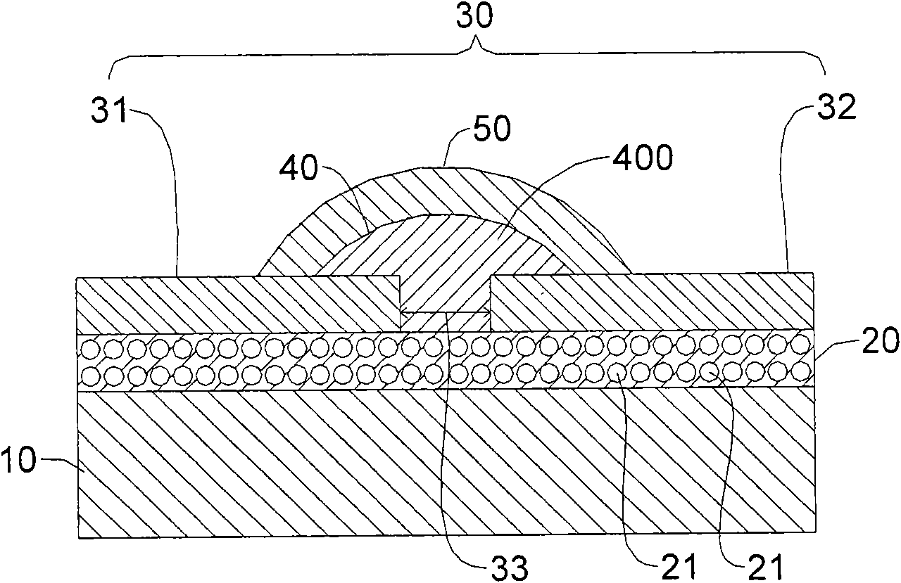
[0044] Such as figure 1 As shown, a specific embodiment of the overvoltage protection device provided by the present invention is disclosed, which mainly includes a substrate 10 , a porous material layer 20 , an electrode layer 30 and a variable impedance material layer 40 .

[0045] The porous material layer 20 is printed on the substrate 10 and has a plurality of through holes 21, and the porous material layer 20 can be a ceramic layer or a polymer layer, but not limited to these two materials.

[0046] The electrode layer 30 is printed on the porous material layer 20 , the electrode layer 30 includes two electrodes 31 , 32 , and the two electrodes 31 , 32 are separated from each other with a distance 33 .

[0047] The variable impedance material layer 40 is printed on the two electrodes 31 , 32 and on the porous material layer 20 within the distance 33 between the two electrodes 31 , 32 .

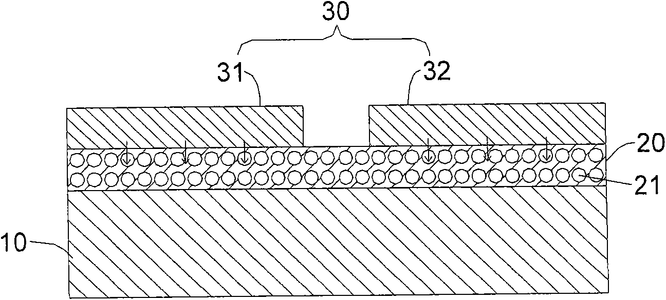
[0048] Such as figure 2As shown, when the aforementioned electrode layer 30 is p...


PUM


Abstract

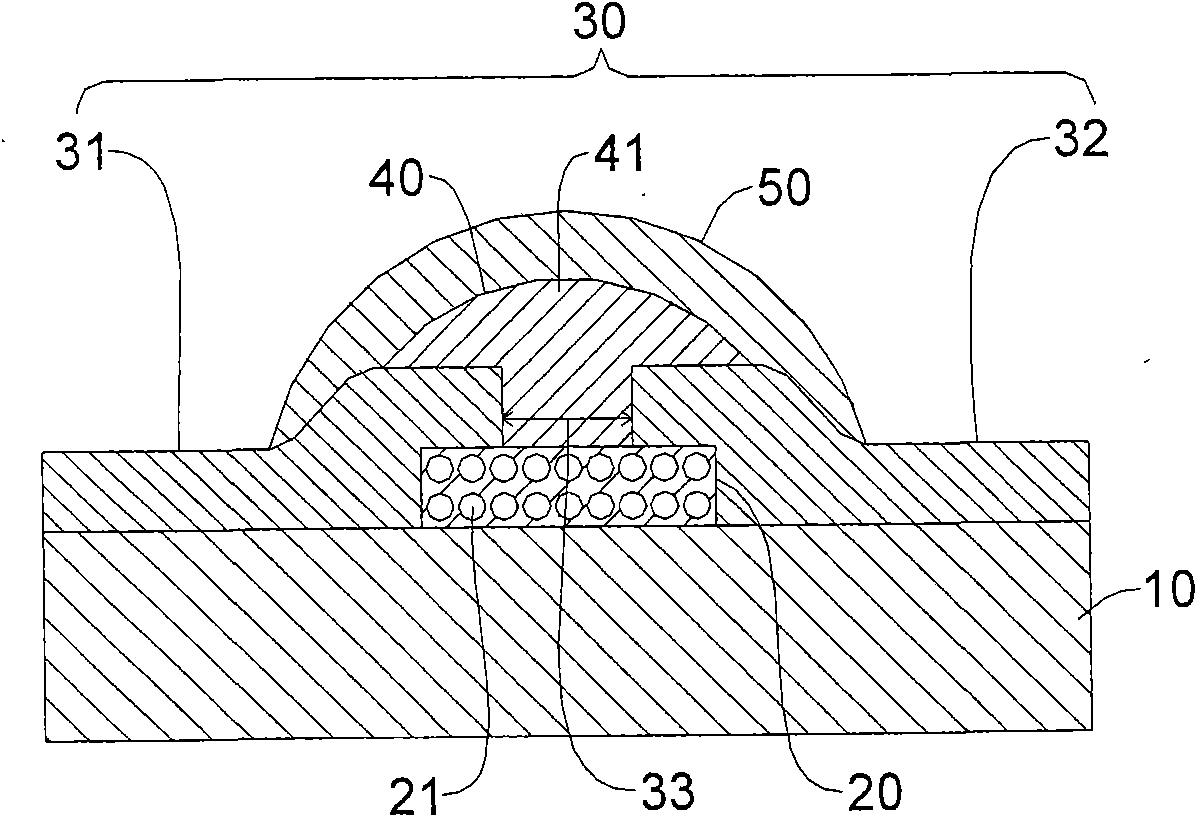
The invention discloses an over-voltage protection element which mainly comprises a substrate, a porous material layer arranged on the substrate, an electrode layer and an adjustable resistance material layer. The porous material layer is provided with a plurality of through holes, and the electrode layer is printed on the porous material layer. When the electrode layer is printed on the porous material layer, supplement sol / solvent and unshaped sol can be rapidly absorbed through the through holes by surface tension so that the electrode layer is fixed and molded and then sintered to prevent the sol of the electrode layer from turning the edges of the electrode layer into acute loss due to naturally dispersing, and further solve the problem of point discharge of the over-voltage protection element. Moreover, the invention has easy, rapid process and no loss of a reduced effective discharging area.

Description

technical field [0001] The invention relates to an overvoltage protection element, especially an overvoltage protection element comprising a porous material layer, the through holes of the porous material layer can absorb excess sol / solvent and unshaped sol in the process through surface tension, and then The electrode layer can be shaped quickly without tip discharge. Background technique [0002] For existing overvoltage protection components see Figure 4 As shown, it mainly includes a substrate 60, a conductive pair 61 and a variable resistance material layer 62, wherein the substrate 60 is a density greater than 3.5g / cm 3 glass or ceramic substrate; the conductive pair 61 is printed on the surface of the substrate 60, the conductive pair 61 includes a signal conductive layer 611 and a ground conductive layer 612 separated from the signal conductive layer 611; the variable impedance material layer 62 It is printed between the signal conductive layer 611 and the ground c...

Claims


Application Information

Patent Timeline
IPC IPC(8): H01C7/12
Inventor 李俊远
Owner THINKING ELECTRONIC IND CO LTD
Learn More